VB024
HIGH VOLTAGE IGNITION COIL DRIVER
POWER IC
s
PRIMARY COIL CURRENT INTERNALLY SET
s
PRIMARY COIL VOLTAGE INTERNALLY SET
s
AUTOMATIC SHUT-OFF AT MAX CURRENT
s
LOGIC LEVEL COMPATIBLE INPUT
s
DIGITAL SIGNAL FEEDBACK TO INDICATE
A PREDETERMINED CURRENT LEVEL
DESCRIPTION
The VB024 is a high voltage integrated circuit
made using SGS-THOMSON VIPower thecnology,
with vertical current flow power darlington and logic
level compatible driving circuit.
The device performs the following functions:
power stage for driving the primary side of the
ignition coil, digital signal feedback to the control
IC to indicate a predetermined current level,
automatic shut-off at maximum current, self
clamping for voltage flyback and logic level input.
September 1993
BLOCK DIAGRAM
ISOWATT7
TYPE
V
CL
I
C
I
d
VB024
400 V
8 A
100 mA
1/8
ABSOLUTE MAXIMUM RATING
Symbol
Parameter
Value
Uni t
HV
C
Collect or Voltage
Internally Limited
V
I
C
Collect or Current
Internally Limited
A
V
d
Driving Stage Supply Voltage
16
V
I
d
Driving Circuitry Supply Current
600
mA
V
in
Maximum Input Voltage
10
V
V
s
Control Circuitry Supply Voltage
8
V
I
s
Control Circuitry Supply Current
200
mA
T
j
Operating Junction Temperature
-40 to 150
o
C
T
stg
St orage Temperat ure Range
-55 to 150
o
C
THERMAL DATA
R
thj-cas e
Thermal Resistance Junction Case
(MAX)
2.5
o
C/ W
R
thj- amb
Thermal Resistance Junction Ambient
(MAX)
30
o
C/ W
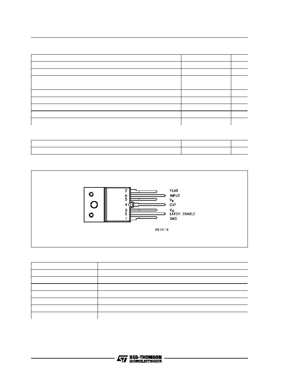
CONNECTION DIAGRAM
PIN FUNCTION
No
NAME
FUNCTI ON
1
GND
Emitt er Power and Control Ground
2
LATCH ENABLE
Enables Of The Latch Circuitry Which Turn Off The Driver
3
Vd
Supply Voltage For The Power Stage
4
OUT
Output to The Primary Coil
5
Vs
Supply Voltage For The Control Stage
6
INPUT
7
FLAG
Output of A Logic Signal When I c I s Greater Than 3 A
VB024
2/8

ELECTRICAL CHARACTERISTICS (V
b
= 12 V; V
s
= 5 V Regulated; T
j
= 25
o
C; R
coil
= 500 m
;
L
coil
= 6mH unless otherwise specified)
Symbol
Parameter
Test Conditi ons
Mi n.
Typ.
Max.
Unit
V
cl
High Volt age Clamp
V
in
= 0.4 V
-40
o
C
T
j
125
o
C
320
510
V
V
ce(sat)
Saturation Voltage of
The Power Stage
I
c
= 6A;
I
d
= 80 mA;
V
in
= 4V
2
V
I
s(on)
Control Circuit Supply
Current
15
mA
V
s
Control Circuit Supply
Voltage
4.5
5.5
V
I
d(on)
Driver Stage Stand-by
Current
V
in
= 4 V
180
mA
V
d
Driver Stage Supply
Voltage
5.5
16
V
I
diag
Diagnostic Current at
Wich The Flag Switches
-40
o
C
T
j
125
o
C
2.75
3.35
mA
V
inH
High Level Input Voltage
4
5.5
V
V
inL
Low Level I nput Volt age
0
0.2
V
I
inH
High Level Input Current V
in
= 5.5 V
20
600
�
A
V
pos
Positive Threshold
2.8
3.2
V
V
neg
Negat ive Threshold
1.3
1.7
V
V
hys
Hysteresis Voltage
1.3
1.7
V
I
c (max)
Turn-Off Current
V
in
= 4 V
-40
o
C
T
j
125
o
C
7.3
8.8
A
t
off
Switch-Off Time
I
c
= 6 A (see note 1)
10
80
�
s
V
diagH
High Level Diagnost ic
Output Voltage
R
flag
= 20 K
4
4.5
V
V
diagL
Low Level Diagnost ic
Output Volatge
R
flag
= 100 K
0.1
V
Note 1: Time fron input swi tching V
ne g
unti l V
CL
dr ops to 200 V
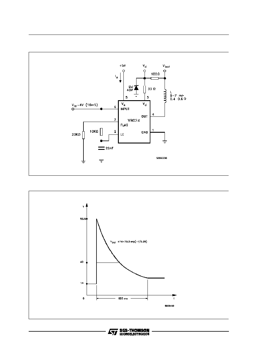
PRINCIPLE OF OPERATION
The VB024 is designed to drive the primary side
of an ignition coil and provide a logic signal
output to indicate a predetermined coil current
level. This output signal is used to perform dwell
control. This part is intended for use in Engine
Control Modules. It could also be used in an
ignition module or integrated into an ignition coil
assembly.
The VB024 accepts an input High signal from the
control IC to start charging the primary side of the
ignition coil. When the primary coil current
reaches 3 amps, the VB024 outputs a logic High
signal to the control IC. This flag signal is used in
the calculation of the dwell time.
This device also has a maximum primary coil
current I
c(max)
Shut-off feature. I
c(max)
equals
aproximately 1.5 times the nominal primary coil
currnet. If the Ic reaches I
c(max)
, the output stage
will Shut-off causing the spark to occour.
The VB024 is also internally clamped to protect it
from
the
flyback
voltage
of
the
primary
inductance as the output stage is turned off.
OVERVOLTAGE
The VB024 withstand the following transient test
performed using a "Schaffner" equipment at T
A
=
80
o
C:
1) LOAD DUMP
Ten pulses with 10 second intervals between
each transient. The device withstand load dump
while fully on, fully off and during the transition
between states (see figures 3 and 4).
2) NEGATIVE TRANSIENTS
Ten negative transients with 10 second intervals
between each transient (see figure 5).
3) REVERSE BATTERY
Inversion of battery voltage for a time = 60 sec
(see figure 5).
VB024
3/8