TSH321
WIDE BANDWIDTH AND MOS INPUTS
SINGLE OPERATIONAL AMPLIFIER
June 1998
®
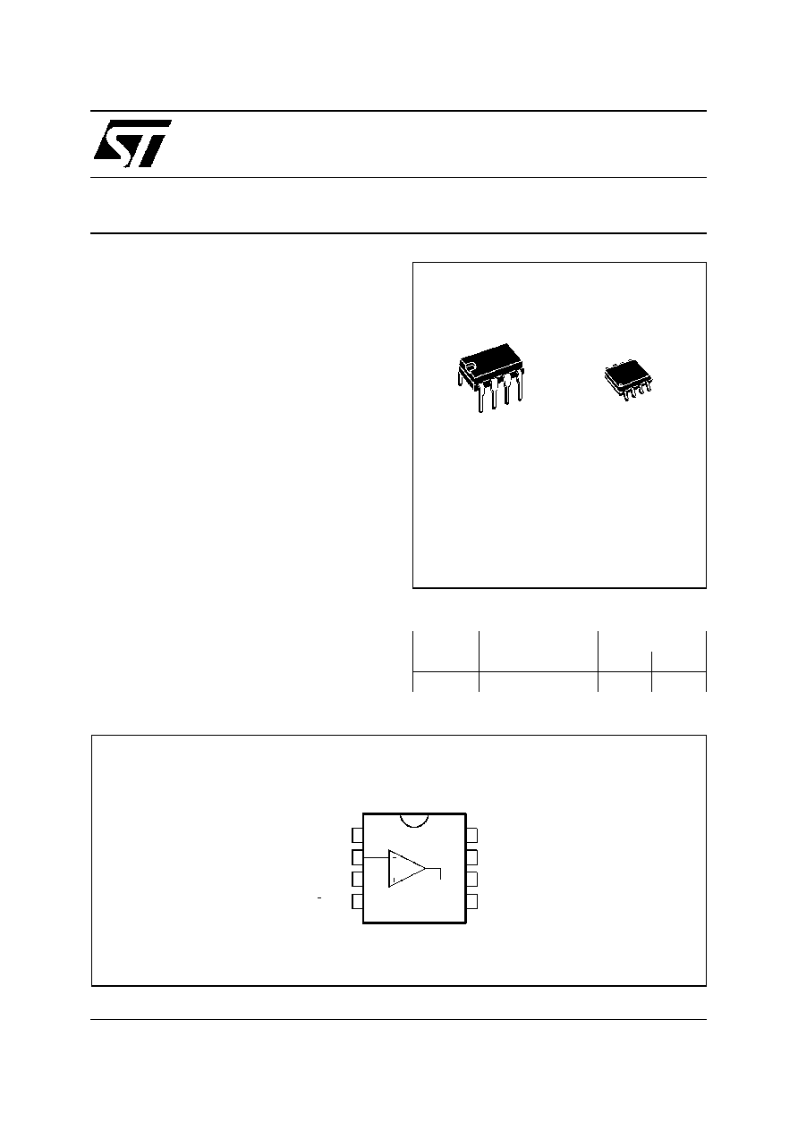
ORDER CODES
Part
Number
Temperature
Range
Package
N
D
TSH321I
-40
o
C, 125
o
C
·
·
321-01.TBL
1
2
3
4
8
6
5
7
Inverting Input
Non-inverting Input
Output
Offset Null 2
Offset Null 1
N.C.
V
CC
V
CC
+
321-01.EPS
PIN CONNECTIONS (top view)
.
LOW DISTORTION
.
GAIN BANDWIDTH PRODUCT : 300MHz
.
GAIN OF 2 STABILITY
.
SLEW RATE : 400V/
µ
s
.
VERY FAST SETTLING TIME : 60ns (0.1%)
.
VERY HIGH INPUT IMPEDANCE
D
SO8
(Plastic Micropackage)
N
DIP8
(Plastic Package)
DESCRIPTION:
The TSH321 is a wideband monolithic operational
amplifier, requiring a minimum close loop gain of 2
for stability.
The TSH321 features extremely high input imped-
ance (typically greater than 10
12
) allowing direct
interfacing with high impedance sources.
Low distortion, wide bandwidth and high linearity
make this amplifier suitable for RF and video appli-
cations. Short circuit protection is provided by an
internal current-limiting circuit.
The TSH321 has internal electrostatic discharge
(ESD) protection circuits and fulfills MILSTD883C-
Class2.
1/6
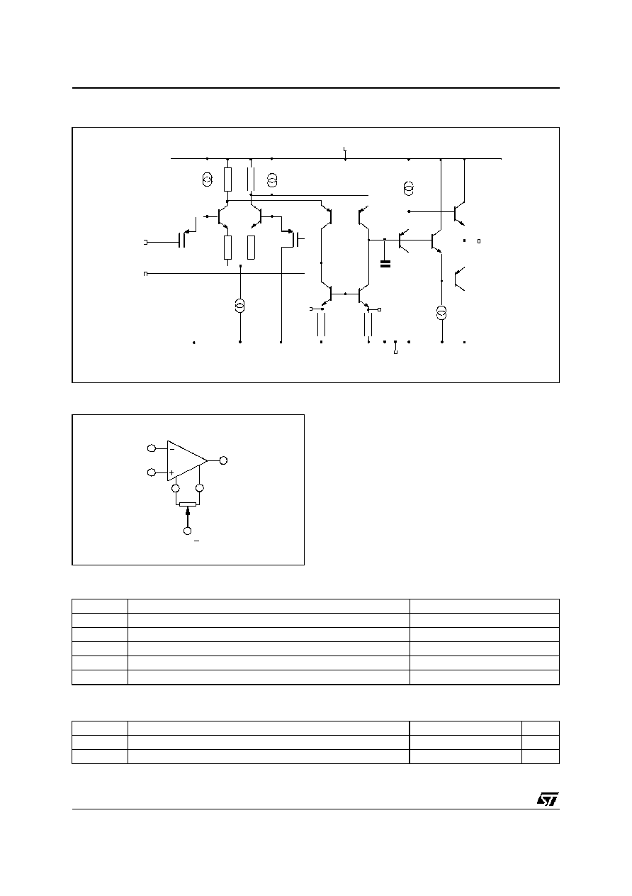
3
non inverting
input
2
inverting
input
1
8
Offset N1
Offset N2
7 V
CC
+
C
c
6
output
Internal
V
CC
-
4
V
ref
321-02.EPS
SCHEMATIC DIAGRAM
ABSOLUTE MAXIMUM RATINGS
Symbol
Parameter
Value
Unit
V
CC
Supply Voltage
±
7
V
V
id
Differential Input Voltage
±
5
V
V
i
Input Voltage Range
±
5
V
I
in
Current On Offset Null Pins
±
20
mA
T
oper
Operating Free-Air Temperature Range
TSH321I
-40
o
C, 125
o
C
o
C
321-02.TBL
N1
N 2
TSH321
100k
V
CC
321-03.EPS
INPUT OFFSET VOLTAGE NULL CIRCUIT
OPERATING CONDITIONS
Symbol
Parameter
Value
Unit
V
CC
Supply Voltage
±
3 to
±
6
V
V
ic
Common Mode Input Voltage Range
V
CC
-
to V
CC
+
-3
V
321-03.TBL
TSH321
2/6
ELECTRICAL CHARACTERISTICS
V
CC
=
±
5V, T
amb
= 25
o
C (unless otherwise specified)
Symbol
Parameter
Min.
Typ.
Max.
Unit
V
io
Input Offset Voltage
T
min
T
amb
T
max.
0.5
10
12
mV
DV
io
Input Offset Voltage Drift
T
min
T
amb
T
max.
10
µ
V/
o
C
I
ib
Input Bias Current
2
300
pA
I
io
Input Offset Current
2
200
pA
I
CC
Supply Current, no load
V
CC
=
±
5V
V
CC
=
±
3V
V
CC
=
±
6V
T
min
T
amb
T
max.
V
CC
=
±
5V
23
21
25
30
28
40
32
mA
A
vd
Large Signal Voltage Gain
V
o
=
±
2.5V
R
L
=
R
L
= 100
R
L
= 50
800
300
200
1300
850
650
V/V
V
icm
Input Common Mode Voltage Range
-5 to +2
-5.5 to +2.5
V
CMR
Common Mode Rejection Ratio
V
ic
= V
icm min.
60
100
dB
SVR
Supply Voltage Rejection Ratio
V
CC
=
±
5V to
±
3V
50
70
dB
V
o
Output Voltage
R
L
= 100
R
L
= 50
T
min
T
amb
T
max.
R
L
= 100
R
L
= 50
±
3
±
2.8
±
2.9
±
2.7
+3.5
-3.7
+3.3
-3.5
V
I
o
Output Short Circuit Current
V
id
=
±
1V, V
o
= 0V
±
50
±
100
mA
GBP
Gain Bandwidth Product
A
VCL
= 100, R
L
= 100
, C
L
= 15pF, f = 7.5MHz
300
MHz
SR
Slew Rate
V
in
=
±
1V, A
VCL
= 2 R
L
= 100
, C
L
= 15pF
200
400
V/
µ
s
e
n
Equivalent Input Voltage Noise
R
S
= 50
fo = 1kHz
fo = 10kHz
fo = 100kHz
fo = 1MHz
20
18.2
18.1
18.2
nV
Hz
K
ov
Overshoot
V
in
=
±
1V A
VCL
= 2, R
L
= 100
, C
L
= 15pF
15
%
t
s
Settling Time 0.1% - (note 1)
V
in
=
±
1V, A
VCL
= -1
60
ns
t
r
, t
f
Rise and Fall Time - (note 1)
V
in
=
±
100mV, A
VCL
= 2
2
ns
t
d
Delay Time - (note 1)
V
in
=
±
100mV, A
VCL
= 2
2
ns
m
Phase Margin
A
VM
= 2, R
L
= 100
,
C
L
= 15pF
45
Degrees
THD
Total Harmonic Distortion
A
VCL
= 10, f = 1KHz, V
o
=
±
2.5V, no load
0.02
%
FPB
Full Power Bandwidth - (note 2)
V
o
= 5Vpp, R
L
= 100
V
o
= 2Vpp, R
L
= 100
26
64
MHz
Note 1 :
See test waveform figure
Note 2 :
Full power bandwidth =
SR
V
opp
321-04.TBL
TSH321
3/6

V
in
50%
t
d
t
r
90%
t
s
0.1% of edge amplitude
10%
321-04.EPS
TEST WAVEFORM
Input
50
1k
1k
10nF
10
µ
F
C
F
-5V
+5V
10nF
10
µ
F
50
Output
321-05.EPS
EVALUATION CIRCUIT
As for any high frequency device, a few rules must
be observed when designing the PCB to get the best
performances from this high speed op amp.
From the most to the least important points :
·
Each power supply lead has to be bypassed
to ground with a 10nF ceramic capacitor very
close to the device and a 10
µ
F tantalum ca-
pacitor.
·
To provide low inductance and low resistance
common return, use a ground plane or com-
mon point return for power and signal.
·
All leads must be wide and as short as possi-
ble especially for op amp inputs. This is in
order to decrease parasitic capacitance and
inductance.
·
Use small resistor values to decrease time
constant with parasitic capacitance.
·
Choose component sizes as small as possible
(SMD).
·
On output, decrease capacitor load so as to
avoid circuit stability being degraded which
may cause oscillation. One can also add a
serial resistor in order to minimise its influ-
ence.
·
One can add in parallel with feedback resistor
a few pF ceramic capacitor C
F
adjusted to
optimize the settling time.
PRINTED CIRCUIT LAYOUT
TSH321
4/6

PM-DIP8.EPS
PACKAGE MECHANICAL DATA
8 PINS - PLASTIC DIP
Dimensions
Millimeters
Inches
Min.
Typ.
Max.
Min.
Typ.
Max.
A
3.32
0.131
a1
0.51
0.020
B
1.15
1.65
0.045
0.065
b
0.356
0.55
0.014
0.022
b1
0.204
0.304
0.008
0.012
D
10.92
0.430
E
7.95
9.75
0.313
0.384
e
2.54
0.100
e3
7.62
0.300
e4
7.62
0.300
F
6.6
0260
i
5.08
0.200
L
3.18
3.81
0.125
0.150
Z
1.52
0.060
DIP8.TBL
TSH321
5/6