THD200FI
HIGH VOLTAGE FAST-SWITCHING
NPN POWER TRANSISTOR
s
STMicroelectronics PREFERRED
SALESTYPE
s
HIGH VOLTAGE CAPABILITY
s
VERY HIGH SWITCHING SPEED
s
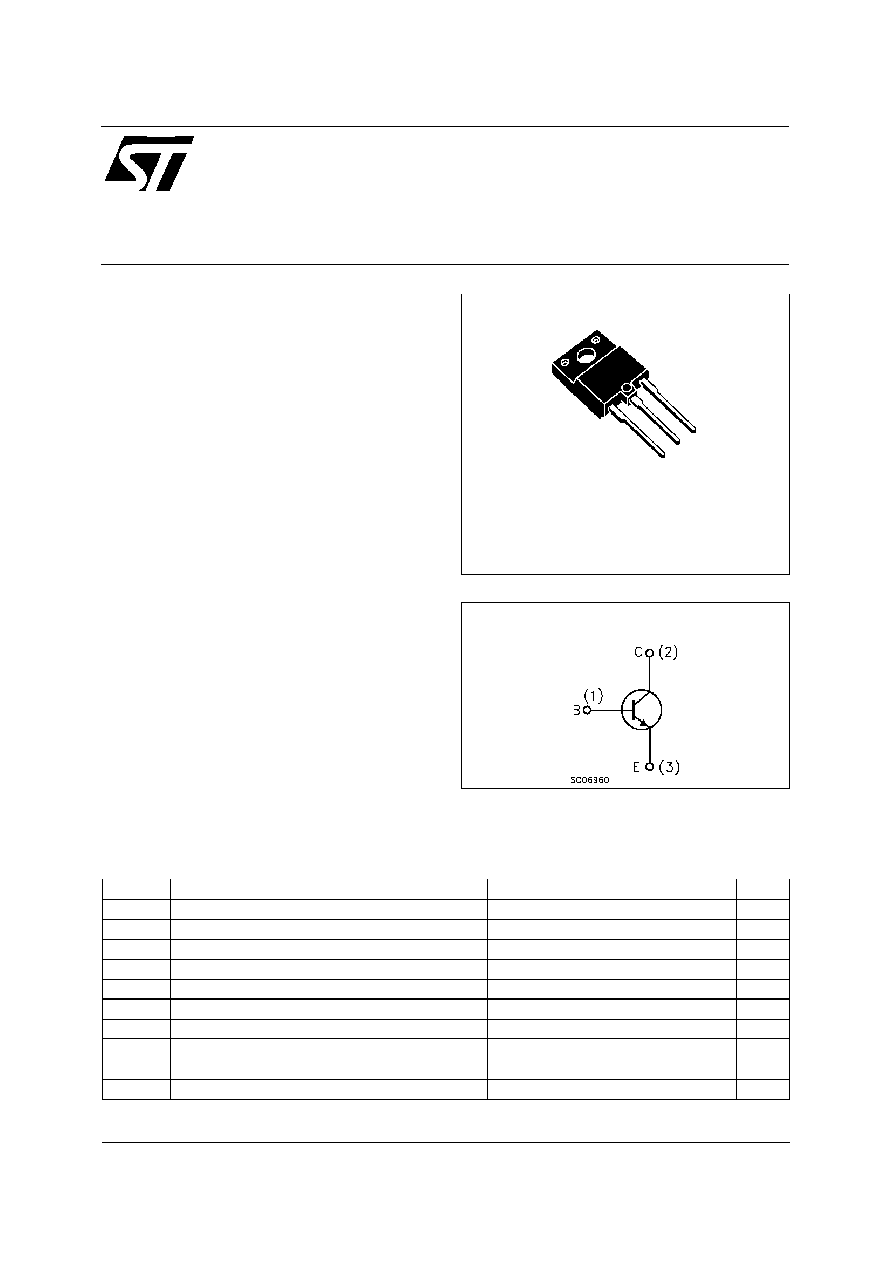
U.L. RECOGNISED ISOWATT218 PACKAGE
(U.L. FILE # E81734 (N))
APPLICATIONS:
s
HORIZONTAL DEFLECTION FOR
MONITORS
DESCRIPTION
The
THD200FI
is
manufactured
using
Multiepitaxial Mesa technology for cost-effective
high performance and uses a Hollow Emitter
structure to enhance switching speeds.
The THD series is designed for use in horizontal
deflection circuits in televisions and monitors.
INTERNAL SCHEMATIC DIAGRAM
December 1999
ABSOLUTE MAXIMUM RATINGS
Symbol
Parameter
Val ue
Uni t
V
CBO
Collect or-Base Voltage (I
E
= 0)
1500
V
V
CEO
Collect or-Emitt er Voltage (I
B
= 0)
700
V
V
EBO
Emitt er-Base Voltage (I
C
= 0)
10
V
I
C
Collect or Current
10
A
I
CM
Collect or Peak Current (t
p
< 5 ms)
20
A
I
B
Base Current
5
A
I
BM
Base Peak Current (t
p
< 5 ms)
10
A
P
t ot
Total Dissipation at T
c
= 25
o
C
57
W
T
stg
St orage Temperature
-65 to 150
o
C
T
j
Max. Operating Junction Temperature
150
o
C
1
2
3
ISOWATT218
®
1/7

THERMAL DATA
R
t hj-ca se
Thermal Resistance Junction-case
Max
2.2
o
C/W
ELECTRICAL CHARACTERISTICS (T
case
= 25
o
C unless otherwise specified)
Symb ol
Parameter
Test Cond ition s
Mi n.
Typ .
Max.
Un it
I
CES
Collect or Cut-off
Current (V
BE
= 0)
V
CE
= 1500 V
V
CE
= 1500 V
T
j
= 125
o
C
0.2
2
mA
mA
I
EBO
Emitt er Cut-off Current
(I
C
= 0)
V
EB
= 5 V
100
µ
A
V
CEO(sus )
Collect or-Emitter
Sustaining Voltage
(I
C
= 0)
I
C
= 100 mA
700
V
V
EBO
Emitt er-Base Voltage
(I
B
= 0)
I
E
= 10 mA
10
V
V
CE(sat )
Collect or-Emitter
Saturat ion Voltage
I
C
= 7 A
I
B
= 1.5 A
1.5
V
V
BE(s at)
Base-Emitt er
Saturat ion Voltage
I
C
= 7 A
I
B
= 1.5 A
1.3
V
h
FE
DC Current G ain
I
C
= 7 A
V
CE
= 5 V
I
C
= 7 A
V
CE
= 5 V
T
j
= 100
o
C
6. 5
4
13
t
s
t
f
RESI STIVE LO AD
St orage Time
Fall T ime
V
CC
= 400 V
I
C
= 7 A
I
B1
= 1.5 A
I
B2
= 3.5 A
2.1
140
3.1
210
µ
s
ns
t
s
t
f
INDUCTIVE LOAD
St orage Time
Fall T ime
I
C
= 7 A
f = 31250 Hz
I
B1
= 1.5 A
I
B2
= -3. 5 A
V
c eflybac k
= 1200 sin
5
10
6
t
V
3.5
320
µ
s
ns
t
s
t
f
INDUCTIVE LOAD
St orage Time
Fall T ime
I
C
= 7 A
f = 64 KHz
I
B1
= 1.5 A
I
B2
= -3. 5 A
V
c eflybac k
= 1200 sin
5
10
6
t
V
1.7
215
µ
s
ns
Pulsed: Pulse duration = 300
µ
s, duty cycle 1.5 %
THD200FI
2/7
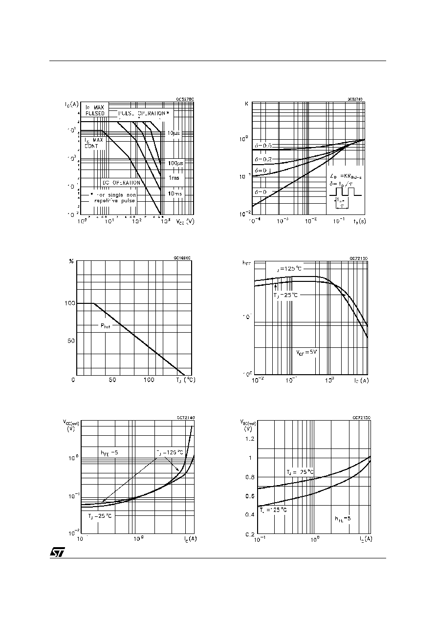
Safe Operating Area
Derating Curve
Collector Emitter Saturation Voltage
Thermal Impedance
DC Current Gain
Base Emitter Saturation Voltage
THD200FI
3/7
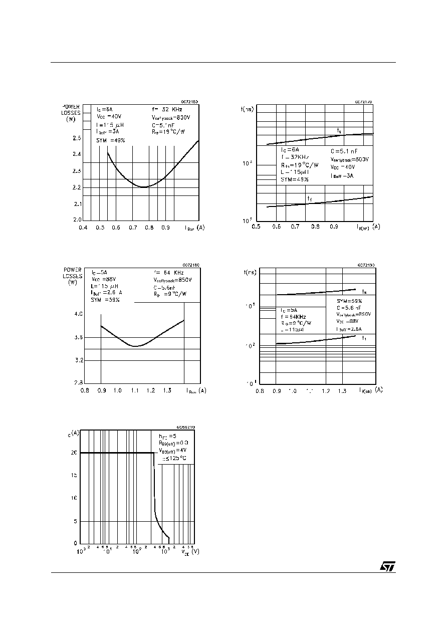
Power Losses at 32 KHz
Power Losses at 64 KHz
Reverse Biased SOA
Switching Time Inductive Load at 32 KHz
(see figure 2)
Switching Time Inductive Load at 64 KHz
(see figure 2)
THD200FI
4/7
In order to saturate the power switch and reduce
conduction losses, adequate direct base current
I
B1
has to be provided for the lowest gain h
FE
at T
j
= 100
o
C (line scan phase). On the other hand,
negative base current I
B2
must be provided turn
off the power transistor (retrace phase). Most of
the
dissipation, especially in
the
deflection
application, occurs at switch-off so it is essential
to determine the value of I
B2
which minimizes
power losses, fall time t
f
and, consequently, T
j
. A
new set of curves have been defined to give total
power losses, t
s
and t
f
as a function of I
B2
at both
32 KHz and 64 KHz scanning frequencies in
order to choice the optimum negative drive. The
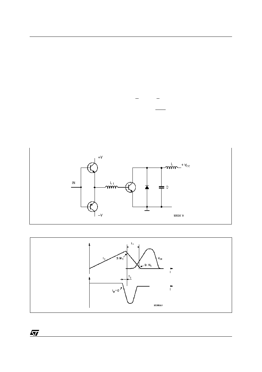
test circuit is illustrated in fig. 1.
Inductance L
1
serves to control the slope of the
negative base current I
B2
in order to recombine
the excess carriers in the collector when base
current is still present, thus avoiding any tailing
phenomenon in the collector current.
The values of L and C are calculated from the
following equations:
1
2
L
(
I
C
)
2
=
1
2
C
(
V
CEfly
)
2
=
2
f
=
1
L
C
Where I
C
= operating collector current, V
CEfly
=
flyback voltage, f= frequency of oscillation during
retrace.
BASE DRIVE INFORMATION
Figure 1: Inductive Load Switching Test Circuit.
Figure 2: Switching Waveforms in a Deflection Circuit.
THD200FI
5/7
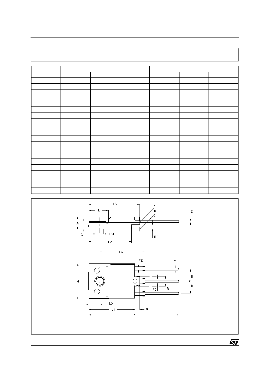
DIM.
mm
inch
MIN.
TYP.
MAX.
MIN.
TYP.
MAX.
A
5.35
5.65
0.211
0.222
C
3.30
3.80
0.130
0.150
D
2.90
3.10
0.114
0.122
D1
1.88
2.08
0.074
0.082
E
0.75
0.95
0.030
0.037
F
1.05
1.25
0.041
0.049
F2
1.50
1.70
0.059
0.067
F3
1.90
2.10
0.075
0.083
G
10.80
11.20
0.425
0.441
H
15.80
16.20
0.622
0.638
L
9
0.354
L1
20.80
21.20
0.819
0.835
L2
19.10
19.90
0.752
0.783
L3
22.80
23.60
0.898
0.929
L4
40.50
42.50
1.594
1.673
L5
4.85
5.25
0.191
0.207
L6
20.25
20.75
0.797
0.817
N
2.1
2.3
0.083
0.091
R
4.6
0.181
DIA
3.5
3.7
0.138
0.146
P025C/A
ISOWATT218 MECHANICAL DATA
- Weight : 4.9 g (typ.)
- Maximum Torque (applied to mounting flange) Recommended: 0.8 Nm; Maximum: 1 Nm
- The side of the dissipator must be flat within 80
µ
m
THD200FI
6/7

Information furnished is believed to be accurate and reliable. However, STMicroelectronics assumes no responsibility for the consequences
of use of such information nor for any infringement of patents or other rights of third parties which may result from its use. No license is
granted by implication or otherwise under any patent or patent rights of STMicroelectronics. Specification mentioned in this publication are
subject to change without notice. This publication supersedes and replaces all information previously supplied. STMicroelectronics products
are not authorized for use as critical components in life support devices or systems without express written approval of STMicroelectronics.
The ST logo is a trademark of STMicroelectronics
©
1999 STMicroelectronics Printed in Italy All Rights Reserved
STMicroelectronics GROUP OF COMPANIES
Australia - Brazil - China - Finland - France - Germany - Hong Kong - India - Italy - Japan - Malaysia - Malta - Morocco -
Singapore - Spain - Sweden - Switzerland - United Kingdom - U.S.A.
http://www.st.com
.
THD200FI
7/7