
TEA7530
MONITOR AMPLIFIER
PRELIMINARY DATA
LOW VOLTAGE
POWER: 100mW AT 5V
ANTIDISTORTION SYSTEM FOR LOW CUR-
RENT LINES
DESCRIPTION
This 8 pins IC is designed for monitor telephone
set and provides:
a) Signal amplification for monitoring
b) Antidistortion by automatic gain adaptation.
June 1993
This is advanced information on a new product now in development or undergoing evaluation. Details are subject to change without notice.
ABSOLUTE MAXIMUM RATINGS
Symbol
Parameter
Value
Unit
Minidip
SO
T
op
Temperature Range
-20 to +70
-20 to +70
°
C
V
LS
Supply Voltage
6
6
V
I
LS
Supply Current for T > 300ms
for T
300ms
90
150
75
120
mA
mA
MINIDIP
SO-8
ORDERING NUMBERS:
TEA7530DP
TEA7530FP
BLOCK DIAGRAM
1/11

FUNCTIONAL DESCRIPTION
TEA7530 performs the following functions:
The circuit amplifies the incoming signal and
feeds it to the loudspeaker.
The Antidistortion system is incorporated for
low current available from line.
The maximum power available on a 50
im-
pedance loudspeaker is 25mW at 3V and 100mW
at 5V.
PIN FUNCTION
N
°
Symbol
Description
1
GND
Ground
2
ADS
Antidistortion
3
V
LS
Supply
4
INP
Input Signal
5
LS1
Output Loudspeaker 1
6
V
REF
Internal Reference Voltage
7
LS2
Output Loudspeaker 2
8
ADJ
Adjust Internal Reference V
LS
ELECTRICAL CHARACTERISTICS (T
amb
= 25
°
C, I
LS
= 30mA unless otherwise specified)
Symbol
Parameter
Test Condition
Min.
Typ.
Max.
Unit
V
LS1
V
LS1
Supply
ILS = 2mA (fig. 5)
I
LS
= 30mA (fig. 5)
2.7
3
3.15
3.3
3.4
V
V
V
LSM
V
LS
Maximum
I
pin8
= 40
µ
A (fig. 5; So = closed)
5.7
V
V
ADJ
Voltage Pin 8
I
LS
= 2 to 30mA (fig. 5
1.0
1.25
1.5
V
G
Loudspeaker Amplifier
Gain
=
V
(
5
)
-
V
(
7
)
V
(
4
)
I
LS
= 30mA (fig. 6)
30
32
34
dB
THD
Distortion
f = 300Hz to 2KHz
V
(5 )
- V
(7 )
= 0.8Vrms; (fig. 6)
2
%
Z
INPIN
Earphone Input
(fig. 7)
2.1
2.8
3.5
K
V
OFFS
Output Offset [V
(5)
- V
(7)
]
(fig. 6)
-80
80
mV
GATT
Loudspeaker Attenuated
Gain = [V
(5 )
- V
(7 )
] / V
(4)
V
(2 )
= 0.7V; (fig. 8)
V
(2 )
= 0.4V; (fig. 8)
20
-30
30
-20
dB
dB
PIN CONNECTION (top view)
TEA7530
2/11

Figure 1: Loudspeaker Gain vs. Voltage on Pin 2
Figure 2: Power Available on Loudspeakervs.
V
LS
Typical Curve. (Voltage Mode
Figure 3: Distortion vs. Output Power
Figure 4: Output Power vs. Supply Current
(Current Mode Supply)
TEA7530
3/11

TEST CIRCUITS
Figure 5: Shuntvoltage Regulator / Reference
Voltage at Pin 8.
Figure 6: Loudspeaker Amplifier:
Gain/Distortion/Output Offset
Figure 7: Impedance, ZINP
Figure 8: Anti-loading Feedback System at
G = GATT
TEA7530
4/11
CIRCUIT DESCRIPTION
TEA7530 is a 8 pin DIP integrated circuit provid-
ing the following facilities:
Loudspeaker amplifier
Antidistortion feed-back system (limited line
current compensation)
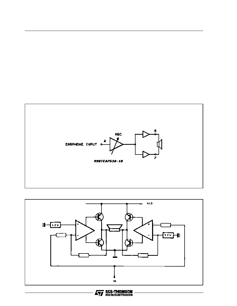
1.1. LOUDSPEAKER AMPLIFIER
The amplifier is divided into 2 main sections.
- Automatic Gain Control (AGC)
- Push-pull amplifier (bridge structure)
a) The AGC section is used for the antidistortion
system.
When used in a telephone set to avoid larsen
effect the AGC automatically decreases loud-
speaker amplifier gain.
When the required output level exceeds the
capabilities of the available current, the AGC
decreases the loudspeaker amplifier gain to
avoids distortion.
b) The output amplifier uses a double push-pull
configuration (H bridge) to get maximum dynamic
range under limited supply conditions.
Figure 9
Figure 10
TEA7530
5/11