
TDE1897C
TDE1898C
0.5A HIGH-SIDE DRIVER
INDUSTRIAL INTELLIGENT POWER SWITCH
0.5A OUTPUT CURRENT
18V TO 35V SUPPLY VOLTAGE RANGE
INTERNAL CURRENT LIMITING
THERMAL SHUTDOWN
OPEN GROUND PROTECTION
INTERNAL NEGATIVE VOLTAGE CLAMPING
TO V
S
- 45V FOR FAST DEMAGNETIZATION
DIFFERENTIAL INPUTS WITH LARGE COM-
MON MODE RANGE AND THRESHOLD
HYSTERESIS
UNDERVOLTAGE LOCKOUT WITH HYSTERESIS
OPEN LOAD DETECTION
TWO DIAGNOSTIC OUTPUTS
OUTPUT STATUS LED DRIVER
DESCRIPTION
The TDE1897C/TDE1898C is a monolithic Intelli-
gent Power Switch in Multipower BCD Technol-
ogy, for driving inductive or resistive loads. An in-
ternal Clamping Diode enables the fast demag-
netization of inductive loads.
Diagnostic for CPU feedback and extensive use
of electrical protections make this device inher-
ently indistructible and suitable for general pur-
pose industrial applications.
September 2003
®
Minidip SIP9 SO20
ORDERING NUMBERS:
TDE1897CDP TDE1898CSP TDE1897CFP
TDE1898CDP TDE1898CFP
BLOCK DIAGRAM
MULTIPOWER BCD TECHNOLOGY
1/12
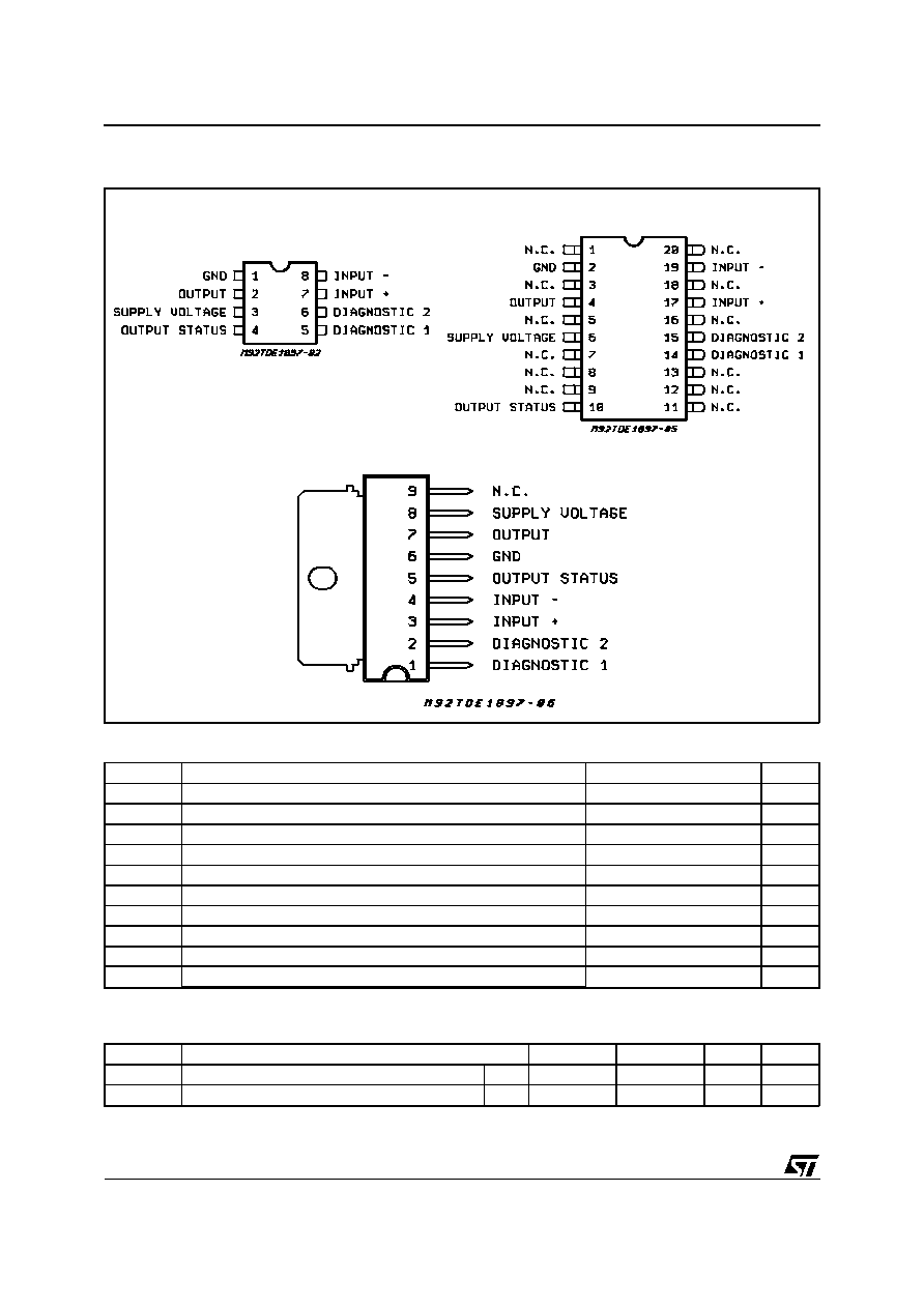
PIN CONNECTIONS (Top view)
ABSOLUTE MAXIMUM RATINGS (Minidip pin reference)
Symbol
Parameter
Value
Unit
V
S
Supply Voltage (Pins 3 - 1) (T
W
< 10ms)
50
V
V
S
V
O
Supply to Output Differential Voltage. See also V
Cl
3-2 (Pins 3 - 2)
internally limited
V
V
i
Input Voltage (Pins 7/8)
-10 to V
S
+10
V
V
i
Differential Input Voltage (Pins 7 - 8)
43
V
I
i
Input Current (Pins 7/8)
20
mA
I
O
Output Current (Pins 2 - 1). See also ISC
internally limited
A
E
l
Energy from Inductive Load (T
J
= 85
°
C)
200
mJ
P
tot
Power Dissipation. See also THERMAL CHARACTERISTICS.
internally limited
W
T
op
Operating Temperature Range (T
amb
)
-25 to +85
°
C
T
stg
Storage Temperature
-55 to 150
°
C
THERMAL DATA
Symbol
Description
Minidip
Sip SO20
Unit
R
th j-case
Thermal Resistance Junction-case
Max.
10
°
C/W
R
th j-amb
Thermal Resistance Junction-ambient
Max.
100
70
90
°
C/W
Minidip
SIP9
SO20
TDE1897C - TDE1898C
2/12

ELECTRICAL CHARACTERISTICS (V
S
= 24V; T
amb
= 25 to +85°C, unless otherwise specified)
Symbol
Parameter
Test Condition
Min.
Typ.
Max.
Unit
V
smin
3
Supply Voltage for Valid
Diagnostics
I
diag
> 0.5mA @ V
dg1
= 1.5V
9
35
V
V
s
3
Supply Voltage (operative)
18
24
35
V
I
q
3
Quiescent Current
I
out
= I
os
= 0
V
il
V
ih
2.5
4.5
4
7.5
mA
mA
V
sth1
Undervoltage Threshold 1
(See fig. 1); T
amb
= 0 to +85
°
C
11
V
V
sth2
3
Undervoltage Threshold 2
(See fig. 1); Tamb = 0 to +85
°
C
15.5
V
V
shys
Supply Voltage Hysteresis
(See fig. 1); T
amb
= 0 to +85
°
C
0.4
1
3
V
I
sc
Short Circuit Current
V
S
= 18 to 35V; R
L
= 1
0.75
1.5
A
V
don
3-2
Output Voltage Drop
@ I
out
= 625mA; T
j
= 25
°
C
@ I
out
= 625mA; T
j
= 125
°
C
250
400
425
600
mV
mV
I
oslk
2
Output Leakage Current
@ V
i
= V
il
, V
o
= 0V
300
µ
A
V
ol
2
Low State Out Voltage
@ V
i
= V
il
; R
L
=
0.8
1.5
V
V
cl
3-2
Internal Voltage Clamp (V
S
- V
O
)
@ I
O
= -500mA
45
55
V
I
old
2
Open Load Detection Current
V
i
= V
ih
; T
amb
= 0 to +85
°
C
1
6
mA
V
id
7-8
Common Mode Input Voltage
Range (Operative)
V
S
= 18 to 35V,
V
S
= V
id
7-8 < 37V
7
15
V
I
ib
7-8
Input Bias Current
V
i
= 7 to 15V; In = 0V
700
700
µ
A
V
ith
7-8
Input Threshold Voltage
V+In > VIn
0.8
1.4
2
V
V
iths
7-8
Input Threshold Hysteresis
Voltage
V+In > VIn
50
400
mV
R
id
7-8
Diff. Input Resistance
@ 0 < +In < +16V; In = 0V
@ 7 < +In < 0V; In = 0V
400
150
K
K
I
ilk
7-8
Input Offset Current
V+In = VIn +Ii
0V < V
i
<5.5V Ii
20
75
25
+20
µ
A
µ
A
In = GND +Ii
0V < V+In <5.5V Ii
250
+10
125
+50
µ
A
µ
A
+In = GND +Ii
0V < VIn <5.5V Ii
100
50
30
15
µ
A
µ
A
V
oth1
2
Output Status Threshold 1
Voltage
(See fig. 1)
12
V
V
oth2
2
Output Status Threshold 2
Voltage
(See fig. 1)
9
V
V
ohys
2
Output Status Threshold
Hysteresis
(See fig. 1)
0.3
0.7
2
V
I
osd
4
Output Status Source Current
V
out
> V
oth1
, V
os
= 2.5V
2
4
mA
V
osd
3-4
Active Output Status Driver
Drop Voltage
V
s
V
os
@ I
os
= 2mA;
T
amb
= -25 to 85
°
C
5
V
I
oslk
4
Output Status Driver Leakage
Current
V
out
< V
oth2
, V
os
= 0V
V
S
= 18 to 35V
25
µ
A
V
dgl
5/6
Diagnostic Drop Voltage
D1 / D2 = L @ I
diag
= 0.5mA
D1 / D2 = L @ I
diag
= 3mA
250
1.5
mV
V
I
dglk
5/6
Diagnostic Leakage Current
D1 / D2 =H @ 0 < V
dg
< V
s
V
S
= 15.6 to 35V
25
µ
A
V
fdg
5/6-3
Clamping Diodes at the
Diagnostic Outputs.
Voltage Drop to V
S
@ I
diag
= 5mA; D1 / D2 = H
2
V
Note Vil < 0.8V, Vih > 2V @ (V+In > VIn); Minidip pin reference.
All test not dissipative.
TDE1897C - TDE1898C
3/12

Figure 1
DIAGNOSTIC TRUTH TABLE
Diagnostic Conditions
Input
Output
Diag1
Diag2
Normal Operation
L
H
L
H
H
H
H
H
Open Load Condition (I
o
< I
old
)
L
H
L
H
H
L
H
H
Short to V
S
L
H
H
H
L
L
H
H
Short Circuit to Ground (I
O
= I
SC
) (**) TDE1897C
TDE1898C
H
<H (*)
H
L
H
H
L
H
H
H
H
Output DMOS Open
L
H
L
L
H
L
H
H
Overtemperature
L
H
L
L
H
H
L
L
Supply Undervoltage (V
S
< V
sth1
in the falling phase of the sup-
ply voltage; V
S
< V
sth2
in the rising phase of the supply voltage)
L
H
L
L
L
L
L
L
(*) According to the intervention of the current limiting block.
(**) A cold lamp filament, or a capacitive load may activate the current limiting circuit of the IPS, when the IPS is initially turned on. TDE1897
uses Diag2 to signal such condition, TDE1898 does not.
SOURCE DRAIN NDMOS DIODE
Symbol
Parameter
Test Condition
Min.
Typ.
Max.
Unit
V
fsd
2-3
Forward On Voltage
@ I
fsd
= 625mA
1
1.5
V
I
fp
2-3
Forward Peak Current
t = 10ms; d = 20%
2
A
t
rr
2-3
Reverse Recovery Time
I
f
= 625mA di/dt = 25A/
µ
s
200
ns
t
fr
2-3
Forward Recovery Time
50
ns
THERMAL CHARACTERISTICS (*)
Lim
Junction Temp. Protect.
135
150
°
C
T
H
Thermal Hysteresis
30
°
C
SWITCHING CHARACTERISTICS (V
S
= 24V; R
L
= 48
) (*)
t
on
Turn on Delay Time
100
µ
s
t
off
Turn off Delay Time
20
µ
s
t
d
Input Switching to Diagnostic
Valid
100
µ
s
Note Vil < 0.8V, Vih > 2V @ (V+In > VIn); Minidip pin reference. (*) Not tested.
TDE1897C - TDE1898C
4/12
APPLICATION INFORMATION
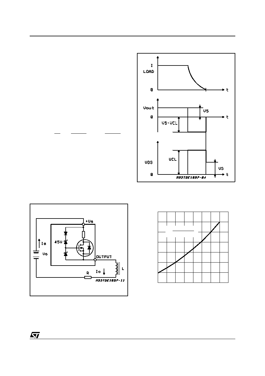
DEMAGNETIZATION OF INDUCTIVE LOADS
An internal zener diode, limiting the voltage
across the Power MOS to between 45 and 55V
(V
cl
), provides safe and fast demagnetization of
inductive loads without external clamping devices.
The maximum energy that can be absorbed from
an inductive load is specified as 200mJ (at
T
j
= 85
°
C).
To define the maximum switching frequency three
points have to be considered:
1) The total power dissipation is the sum of the
On State Power and of the Demagnetization
Energy multiplied by the frequency.
2) The total energy W dissipated in the device
during a demagnetization cycle (figg. 2, 3) is:
W
=
V
cl
L
R
L
[
I
o
V
cl
V
s
R
L
log
1
+
V
s
V
cl
V
s
]
Where:
V
cl
= clamp voltage;
L = inductive load;
R
L
= resistive load;
Vs = supply voltage;
I
O
= I
LOAD
3) In normal conditions the operating Junction
temperature should remain below 125
°
C.
Figure 2: Inductive Load Equivalent Circuit
Figure 3: Demagnetization Cycle Waveforms
-25
0
25
50
75
100
125
Tj (°C)
0.6
0.8
1.0
1.2
1.4
1.6
1.8
D93IN018
=
RDSON (Tj)
RDSON (Tj=25°C)
Figure 4: Normalized R
DSON
vs. Junction
Temperature
TDE1897C - TDE1898C
5/12