1/23
STW81100
October 2005
1
Features
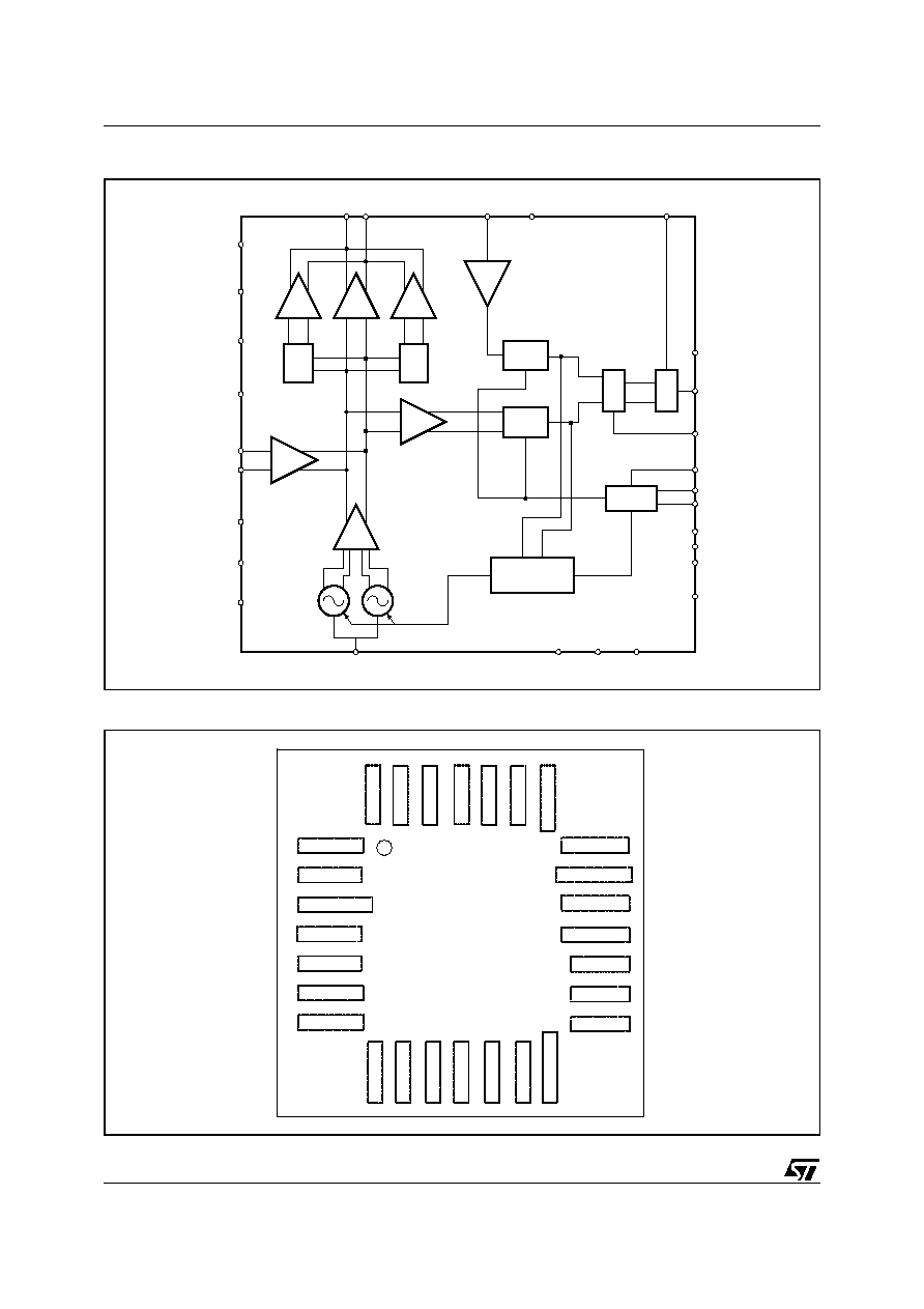
Integer-N Frequency Synthesizer
Dual differential integrated VCOs with
automatic center frequency calibration:
Direct Output:
3300 3900 MHz
3800 4400 MHz
Internal divider by 2:
1650 1950 MHz
1900 2200 MHz
Internal divider by 4:
825 975 MHz
950 1100 MHz
Fast lock time: 150
µs
Dual modulus prescaler (64/65) and 2
programmable counters to achieve a feedback
division ratio from 4096 to 32767.
Programmable reference frequency divider (9
bits)
Phase frequency comparator and charge pump
Programmable charge pump current
Digital Lock Detector
I
2
C bus interface with 3 bit programmable
address (1100A
2
A
1
A
0
)
3.3V Power Supply
Power down mode
Small size exposed pad VFQFPN28 package
5x5x1.0mm
Process: BICMOS 0.35
µm SiGe
2
Description
The STMicroelectronics STW81100 is an integrat-
ed RF synthesizer and voltage controlled oscilla-
tors (VCOs).
Showing high performance, high integration, low
power, and multi-band performances, STW81100
is a low cost one chip alternative to discrete PLL
and VCOs solutions.
STW81100 includes an Integer-N frequency syn-
thesizer and two fully integrated VCOs featuring
low phase noise performance and a noise floor of
-153dBc/Hz. The combination of wide frequency
range VCOs (thanks to center-frequency calibra-
tion over 32 sub-bands) and multiple output op-
tions (direct output, divided by 2 or divided by 4)
allows to cover the 825MHz-1100MHz, the
1650MHz-2200MHz and the 3300MHz-4400MHz
bands.
The STW81100 is designed with STMicroelectron-
ics advanced 0.35
µm SiGe process.
3
Applications
Cellular 3G Infrastructure Equipment
Other Wireless Communication Systems
MULTI-BAND RF FREQUENCY SYNTHESIZER WITH
INTEGRATED VCO
S
Rev. 5
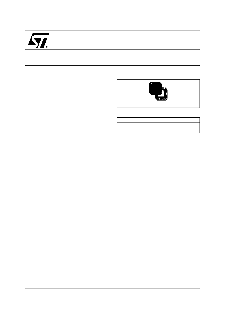
Figure 1. Package
Table 1. Order Codes
Part Number
Package
STW81100AT-1
VFQFPN28
STW81100ATR-1
VFQFPN28 in Tape & Reel
VFQFPN28
3/23
STW81100
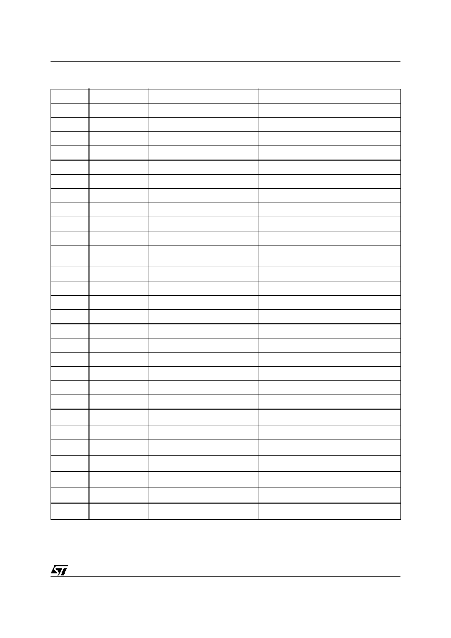
Table 2. Pin Description
Pin No
Name
Description
Observations
1
VDD_VCO1
VCO power supply
2
VDD_DIV2
Divider by 2 power supply
3
VDD_OUTBUF
Output buffer power supply
4
OUTBUFP
LO buffer positive output
Open collector
5
OUTBUFN
LO buffer negative output
Open collector
6
VDD_DIV4
Divider by 4 power supply
7
VDD_VCO2
VCO power supply
8
VDD_ESD
ESD positive rail power supply
9
VCTRL
VCO control voltage
10
ICP
PLL charge pump output
11
REXT
External resistance connection for
PLL charge pump
12
VDD_CP
Power supply for charge pump
13
TEST1
Test input 1
Test purpose only; must be connected to GND
14
LOCK_DET
Lock detector
CMOS Output
15
TEST2
Test input 2
Test purpose only; must be connected to GND
16
REF_IN
Reference frequency input
17
VDD_PLL
PLL digital power supply
18
EXTVCO_INN
External VCO negative input
Test purpose only; must be connected to GND
19
EXTVCO_INP
External VCO positive input
Test purpose only; must be connected to GND
20
VDD_BUFVCO
VCO buffer power supply
21
ATPGON
SCAN mode activated
Test purpose only; must be connected to GND
22
VDD_I
2
C
I
2
C bus power supply
23
EXT_PD
Power down hardware
CMOS Input
24
SDA
I
2
CBUS data line
CMOS Bidir Schmitt triggered
25
SCL
I
2
CBUS clock line
CMOS Input
26
ADD0
I
2
CBUS address select pin
CMOS Input
27
ADD1
I
2
CBUS address select pin
CMOS Input
28
ADD2
I
2
CBUS address select pin
CMOS Input
STW81100
4/23
Table 3. Absolute Maximum Ratings
Note:
1. The maximum rating of the ESD protection circuitry on pin 4 and pin 5 is 800V with respect to other supply pins and 2KV with
respect to ground.
Table 4. Operating Conditions
Table 5. Digital Logic Level
1
Note:
1. All parameters are guaranteed by design and characterization.
4
Electrical Characteristcs
All Electrical Specifications are intended at 3.3V supply voltage.
Symbol
Parameter
Values
Unit
AV
CC
Analog Supply voltage
0 to 4.6
V
DV
CC
Digital Supply voltage
0 to 4.6
V
T
stg
Storage temperature
+150
°C
ESD
Electrical Static Discharge
- HBM
1
- CDM-JEDEC Standard
2
0.5
KV
Symbol
Parameter
Test conditions
Min
Typ
Max
Unit
AV
CC
Analog Supply voltage
3.0
3.3
3.6
V
DV
CC
Digital Supply voltage
3.0
3.3
3.6
V
I
CC
Current Consumption
100
mA
T
amb
Operating ambient temperature
-40
85
°C
T
j
Maximum junction temperature
125
°C
R
th j-a
Junction to ambient package thermal
resistance
Multilayer JEDEC board
35
°C/W
Symbol
Parameter
Test conditions
Min
Typ
Max
Unit
V
il
Low level input voltage
0.2*Vdd
V
V
ih
High level input voltage
0.8*Vdd
V
V
hyst
Schmitt trigger hysteresis
0.8
V
V
ol
Low level output voltage
0.4
V
V
oh
High level output voltage
0.85*Vdd
V
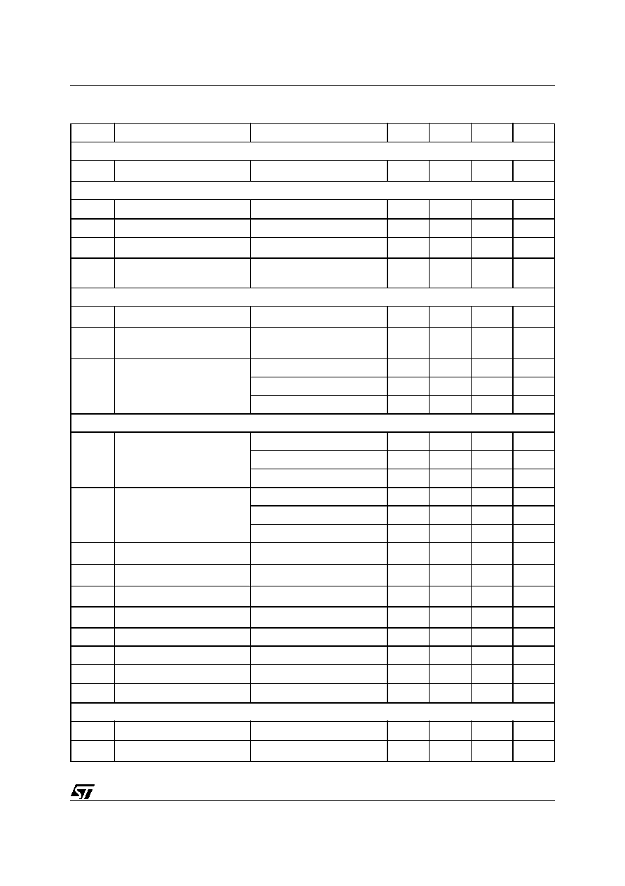
Table 6. Electrical Characteristcs
Symbol
Parameter
Test Condition
Min
Typ
Max
Units
OUTPUT FREQUENCY RANGE
F
OUTA
VCOA Frequency Range
Direct Output
3300
3900
MHz
Divider by 2
1650
1950
MHz
Divider by 4
825
975
MHz
F
OUTB
VCOB Frequency Range
Direct Output
3800
4400
MHz
Divider by 2
1900
2200
MHz
Divider by 4
950
1100
MHz
5/23
STW81100
Symbol
Parameter
Test Condition
Min
Typ
Max
Units
VCO DIVIDERS
N
VCO Divider Ratio
1
4096
32767
REFERENCE and PHASE FREQUENCY DETECTOR
f
ref
Reference input frequency
10
19.2
100
MHz
Reference input sensitivity
0.35
1
1.5
Vpeak
f
PFD
PFD input frequency
4
10
MHz
f
step
Frequency step
1
F
OUT
/
32767
F
OUT
/
4096
Hz
CHARGE PUMP
I
CP
ICP sink/source
2
3bit programmable
4
mA
V
OCP
Output voltage compliance
4
range
0.4
V
dd
-0.3
V
Spurious
3,4
Direct Output
-65
-54
dBc
Divider by 2
-70
-60
dBc
Divider by 4
-70
-66
dBc
VCOs
Kvco
A
VCOA sensitivity
3,4
Sub-Band 00000
85
105
135
MHz/V
Sub-Band 01111
55
70
95
MHz/V
Sub-Band 11111
35
50
65
MHz/V
Kvco
B
VCOB sensitivity
3,4
Sub-Band 00000
60
75
100
MHz/V
Sub-Band 01111
35
45
60
MHz/V
Sub-Band 11111
20
25
35
MHz/V
VCO
A
Pushing
3,4
7
10
MHz/V
VCO
B
Pushing
3,4
9
14
MHz/V
VCO control voltage
4
0.4
3
V
LO Harmonic Spurious
4
-20
dBc
VCO current consumption
25
mA
VCO buffer consumption
15
mA
I
DIV2
DIVIDER by 2 consumption
18
mA
I
DIV4
DIVIDER by 4 consumption
14
mA
LO OUTPUT BUFFER
P
OUT
Output level
0
dBm
RL
Return Loss
4
Matched to 50ohm
15
dB
Table 6. Electrical Characteristcs (continued)