
This is preliminary information on a new product in development or undergoing evaluation. Details are subject to change without notice.
Version 3.0
April 2000
1/38
This is preliminary information on a new product now in development. Details are subject to change without notice.
STV2000
I2C SINGLE FREQUENCY DEFLECTION PROCESSOR AND
70 MHz RGB PREAMPLIFIER
PRELIMINARY DATA
FEATURES
Horizontal deflection
s
Single frequency, self adaptive oscillator.
s
TTL compatible positive going sync.
s
I
2
C
controlled:
H-position,
Pin
Cushion,
Keystone, Parallelogram, Side Pin Balance,H-
amplitude.
s
DC East/West feedback.
s
DC controls: H-width breathing compensation.
s
X-Ray protection
Vertical deflection
s
Vertical ramp generator.
s
Wide range AGC loop.
s
TTL compatible positive going sync, no extra
pulses.
s
I
2
C controls: vertical position and S-correction.
s
DC controls: height breathing compensation.
Video preamplifier
s
3-channel 70MHz bandwidth RGB preamplifier.
s
5ns typical rise and fall time at 4V
PP
.
s
I
2
C controls: RGB contrast, cut-off, brightness,
contrast up-date during vertical retrace time.
s
ABL will reduce gain (contrast).
s
0.514V typical video input signal for normal
display.
I
2
C Main features
s
I
2
C interface (slave) 100kHz max.
s
All I
2
C controlled DAC are 7bit, except for RGB
gain and cut-off.
s
Power- on- reset at 5 V (V
DD
).
s
0.5 to 4 V static DAC output.
Supply voltage & power
s
5 V/10.5 V dual supply.
s
Max power consumption: 1.2W
DESCRIPTION
The STV2000 is an I
2
C-controlled monolithic
integrated circuit assembled in a TQFP44 plastic
package. It combines both a deflection block
(horizontal and vertical, single frequency with very
powerful geometry correction) and a 70MHz RGB
pre-amplifier.
PIN CONNECTIONS
TQFP44
ORDER CODE :
1
2
3
4
5
6
7
8
9
10
11
33
32
31
30
29
28
27
26
25
24
23
44 43 42 41 40 39 38 37 36 35 34
12 13 14 15 16 17 18 19 20 21 22
PGDN
Out3
Cut-off3
PVcc
In1
VBDC
ABLin
In2
DAC
HBRTHin
EWFBin
EW
ou
t
Vout
VBRTHin
AGND
VRB
VAVcc
Out1
Cut-off 1
Out2
Cut-off2
FILTER
PLL2C
HGND
Hfly
Href
SDA
V
DD
(5V)
Hout
LGDN
SAVcc
SCL
VCAP
VGND
VAGCAP
Vref
Hin
FC1
Ro
Co
PLL1F
Vin
N.C.
In3
1

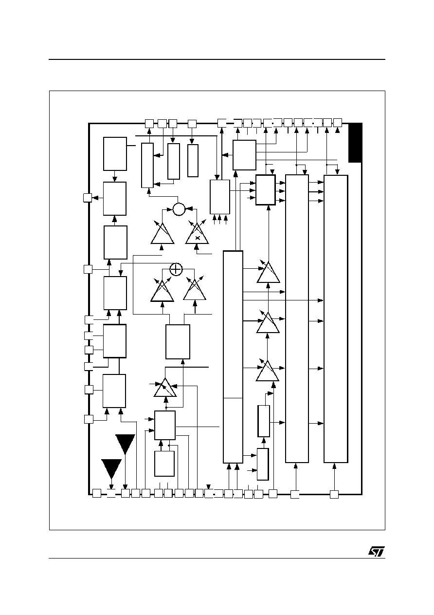
TABLE OF CONTENTS
2
2/38
PIN DESCRIPTION . . . . . . . . . . . . . . . . . . . . . . . . . . . . . . . . . . . . . . . . . . . . . . . . . . . . . . . . . . . . . 3
BLOCK DIAGRAM . . . . . . . . . . . . . . . . . . . . . . . . . . . . . . . . . . . . . . . . . . . . . . . . . . . . . . . . . . . . . . 4
ABSOLUTE MAXIMUM RATINGS . . . . . . . . . . . . . . . . . . . . . . . . . . . . . . . . . . . . . . . . . . . . . . . . . 5
THERMAL DATA . . . . . . . . . . . . . . . . . . . . . . . . . . . . . . . . . . . . . . . . . . . . . . . . . . . . . . . . . . . . . . . 5
SYNC INPUT . . . . . . . . . . . . . . . . . . . . . . . . . . . . . . . . . . . . . . . . . . . . . . . . . . . . . . . . . . . . . . . . . . 5
I2C READ/WRITE . . . . . . . . . . . . . . . . . . . . . . . . . . . . . . . . . . . . . . . . . . . . . . . . . . . . . . . . . . . . . . . 6
HORIZONTAL SECTION . . . . . . . . . . . . . . . . . . . . . . . . . . . . . . . . . . . . . . . . . . . . . . . . . . . . . . . . . 6
VERTICAL SECTION) . . . . . . . . . . . . . . . . . . . . . . . . . . . . . . . . . . . . . . . . . . . . . . . . . . . . . . . . . . . 8
VIDEO PRE-AMP SECTION . . . . . . . . . . . . . . . . . . . . . . . . . . . . . . . . . . . . . . . . . . . . . . . . . . . . . 11
LOGIC SECTION . . . . . . . . . . . . . . . . . . . . . . . . . . . . . . . . . . . . . . . . . . . . . . . . . . . . . . . . . . . . . . 12
I2C BUS ADDRESS TABLE . . . . . . . . . . . . . . . . . . . . . . . . . . . . . . . . . . . . . . . . . . . . . . . . . . . . . 13
TYPICAL OUTPUT WAVEFORMS . . . . . . . . . . . . . . . . . . . . . . . . . . . . . . . . . . . . . . . . . . . . . . . . 15
OPERATING DESCRIPTION . . . . . . . . . . . . . . . . . . . . . . . . . . . . . . . . . . . . . . . . . . . . . . . . . . . . . 19
SCANNING PART . . . . . . . . . . . . . . . . . . . . . . . . . . . . . . . . . . . . . . . . . . . . . . . . . . . . . . . 19
PRE-AMPLIFIER PART . . . . . . . . . . . . . . . . . . . . . . . . . . . . . . . . . . . . . . . . . . . . . . . . . . . 27
STAND-BY MODE AND PROTECTIONS . . . . . . . . . . . . . . . . . . . . . . . . . . . . . . . . . . . . . 31
INTERNAL SCHEMATICS . . . . . . . . . . . . . . . . . . . . . . . . . . . . . . . . . . . . . . . . . . . . . . . . . . . . . . . 32
PACKAGE MECHANICAL DATA . . . . . . . . . . . . . . . . . . . . . . . . . . . . . . . . . . . . . . . . . . . . . . . . . 40
2

STV2000
3/38
PIN DESCRIPTION
Pin
Name
Fun ction
1
Vin
Vertical Sync Input
2
Vref
Vertical Section Reference Voltage
3
VAGCCAP
Vertical AGC Loop Capacitor
4
VGND
Vertical Section Ground
5
VCAP
Vertical Sawtooth Generator Capacitor
6
Vout
Vertical Output
7
VBRTHin
Vertical Breathing DC Input
8
VRB
Vertical Ramp Filter
9
VAVcc
Video Section Analog Supply (10.5V typ)
10
OUT1
Video Output 1
11
Cut-off1
Cut-off1 DAC voltage output pin
12
AGND
Video Analog Ground
13
OUT2
Video Output 2
14
Cutoff2
Cut-off2 DAC voltage output pin
15
PGND
Video Section Power Ground
16
OUT3
Video Output 3
17
Cutoff3
Cut-off3 DAC voltage output pin
18
PVcc
Video Section Power Supply (10.5V typ)
19
IN1
Video Input 1
20
ABLin
Video Automatic Beam Current Compensation Input
21
IN2
Video Input 2
22
DAC
7bits DAC Voltage Output
23
IN3
Video Input 3
24
VBDC
Vertical Blanking Output with DC level adjusted by DAC
25
N.C.
Not to be connected
26
HBRTHin
Horizontal Breathing Compensation DC Input
27
EWFBin
EW Correction Feedback Input
28
EWout
EW Buffer Output
29
V
DD
Bus, Scanning Logic and Video Logic Supply (5V typ)
30
SDA
I
2
C Data Input
31
SCL
I
2
C Clock Input
32
SAVcc
Scanning Section Analog Supply (10.5Vtyp)
33
LGND
Bus and Scanning Power Ground
34
Hout
Horizontal Driver Output, open collector
35
Href
Horizontal Section Reference Voltage
36
Hfly
Horizontal Flyback Input, Positive
37
HGND
Horizontal Section Ground
38
PLL2C
PLL2 Loop Filter
39
Filter
Horizontal Filter Capacitor (HPOS)
40
PLL1F
PLL1 Loop Filter
41
Co
Horizontal Oscillator Capacitor
42
Ro
Horizontal Oscillator Resistor
43
FC1
PLL1 filter capacitor
44
Hin
Horizontal Sync Input
3
S
T
V
200
0
4/
38
BLO
CK
DIAGRAM
PLL1F
Filter
FC1
Ro
Co HFly
PLL2C
Hout
40
39
43
42
41
36
38
34
SAV
CC
Href
Vref
Hin
Vin
HGND
VGND
VCAP
VAGCCAP
VBRTHin
Vout
VRB
SDA
SCL
VDD
LGND
IN1
IN2
IN3 23
21
19
33
29
31
30
8
6
7
3
5
4
37
1
44
2
35
32
Href
Vref
Vpos
Vamp
Scorr
VOSC
RAMP
Generator
Geometry
Tracking
Phase
Freq
Comp
VCO
Phase
Comp
Phase
Shifter
HOUT
Buffer
Safety
SPB
X
2
X
EWPCC
X
2
EW OUTPUT
H Breathing
ABL
Blanking
HFly
Hsync
Vsync
DAC
Output
Stage
BPCP
Drive
Brightness
Contrast
Clamp
Hsync
KeyBal
KEYST
LATCHES & DACs
I
2
C BUS
DECODER
STV2000
17
16
15
14
13
18
11
10
12
9
+
28 EWout
EWFBin
27
26 HBRTHin
20 ABLin
24 VBDC
22 DAC
VAV
CC
AGND
OUT 1
Cut-off 1
PV
CC
OUT 2
Cut-off 2
PGND
OUT 3
Cut-off 3
3
STV2000
5/38
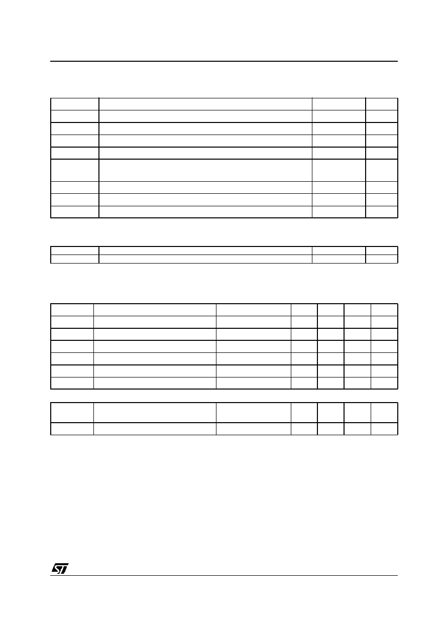
ABSOLUTE MAXIMUM RATINGS
THERMAL DATA
SYNC INPUT
Symbol
Parameter
Value
Unit
SAVcc
Scanning Section Analog Supply Voltage
13.5
V
VAVcc
Video Section Analog Supply Voltage
13.5
V
PVcc
Supply Voltage for Video Pre-Amp Section
13.5
V
Vdd
Logic Section Supply Voltage
5.5
V
V
ESD
ESD susceptibility HBM model 100pF & 1.5k
EIAJ Norm 200pF & 0
2
300
kV
V
Tstg
Storage Temperature
-40 to 150
o
C
Tj
Junction Temperature
150
o
C
Toper
Operating Temperature (Device ambient)
0 to 70
o
C
Symbol
Parameter
Value
Unit
R
TH(j-a)
Junction to Ambient Thermal Resistance (MAX)
46
o
C/W
Operating Conditions (V
DD
= 5V, T
amb
= 25
°
C)
Symbol
Parameter
Test Conditi ons
Min
Typ
Max
Unit
HSVR
Voltage on Hin
Pin 44
0
5
V
MinD
Min Hin pulse duration
Pin 44
0.7
us
Mduty
Max Hin Duty Cycle
Pin 44
25
%
VSVR
Voltage on Vin
Pin 1
0
5
V
VSW
Min Vin pulse duration
Pin 1
5
us
VSD
Max Vin Duty Cycle
Pin 1
15
%
Electrical Characteristics (V
DD
= 5V, T
amb
= 25
°
C)
V
INTH
Horizontal & Vertical Input Logic Level
Low Level
High Level
2.2
0.8
V
V
RIN
Horizontal & Vertical Pull-Up Resistor
200
k
4