STU2071
4B3T U INTERFACE CIRCUIT
PRELIMINARY DATA
4B3T TWO-WIRE U INTERFACE CIRCUIT
FOR LT AND NT APPLICATION
120 kbaud LINE SYMBOL RATE (120 SYM-
BOLS PER FRAME)
SCRAMBLER AND DESCRAMBLER AC-
CORDING TO CCITT REC V.29
BARKER CODE (11 SYMBOLS) SYNCHRO-
NIZATION WORD
UNSCRAMBLED 1 KBIT/S HOUSEKEEPING
CHANNEL
ADAPTIVE ECHO CANCELLATION WITH
TRANSVERSAL FILTERING
ADAPTIVE DECISION FEEDBACK EQUALI-
ZATION
AUTOMATIC GAIN CONTROL
PDM AD CONVERTER
AUTOMATIC ACTIVATION AND DEACTIVA-
TION WITH POLARITY ADAPTION
AUTOMATIC CODE VIOLATION DETECTION
POWER FEED UNIT CONTROL
ADVANCED CL3 1.5
Á
m CMOS PROCESS
28 PIN DUAL-IN-LINE PLASTIC PACKAGE
V* DIGITAL INTERFACE
SYSTEM OVERVIEW
STU2071 (UIC) provides two transparent 64 kbit/s
B channels, a transparent 16 kbit/s D channel, a
transparent 1 kbit/s service channel and a 1 kbit/s
maintenance channel for loop and error mes-
sages on subscriber lines.
UIC enables full duplex continuous data transmis-
sion via the standard twisted pair telephone ca-
ble. Adaptive Echo cancellation is used to restore
the received data. An equalizer, done with an
adaptive filter, restores the data which are dis-
torted by the transmission line.
The coefficient of the equalizer and echo cancel-
ler are conserved during a power down. An all
digital PLL performs both bit and frame synchroni-
zation.
The analog front end consists of receive path RX
and transmit path TX, providing a full duplex ana-
log interfacing to the twisted pair telephone cable.
Before data are converted to analog signals, they
pass through a digital filter (TX-filter) to reduce
the high frequency components. After D/A con-
version the signal is amplified and sent to the hy-
brid.
The received signal is converted back to digital
data and passed through the RX matching filter to
restore the line signal. The A/D convertor is a
second order sigma/delta modulator which oper-
ates with a clock of 15.36 MHz. After timing re-
covery, achieved by a digital PLL, the received
signal is equalized, in an adaptive digital filter, to
correct for the frequency and group delay distor-
tion of the line.
Power supply status can be read via PFOFF. The
UIC can disable its power supply (DISS), and two
relay drivers outputs are provided (accessible via
B2*) to control the power feed unit (RD1,RD2).
This is advanced information on a new product now in development or undergoing evaluation. Details are subject to change without notice.
September 1994
DIP28
ORDERING NUMBER: STU2071B1
PLCC28
ORDERING NUMBER: STU2071FN
1/18

PIN CONNECTION (Top view)
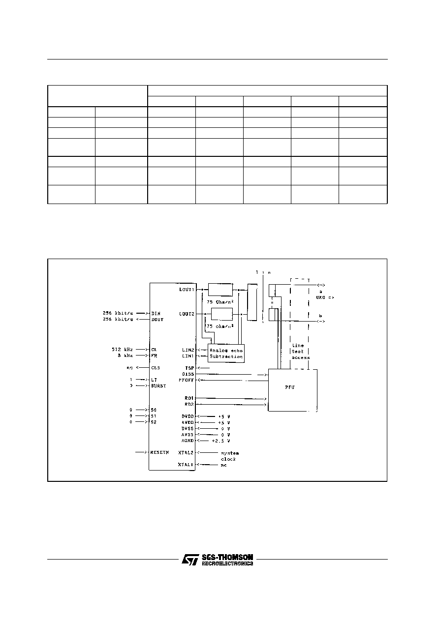
Figure 1: UIC Schematic Block Diagram
1
2
3
4
5
6
7
8
10
9
11
25
24
23
22
20
21
19
26
28
27
15
14
13
12
18
16
17
DVSS
PFOFF
LT
TEST
XTAL1
CLS
XTAL2
DISS/COEF
RESETN
DIN
TSP
FR
BURST
DOUT
LIN2
LIN1
LOUT2
AGND
LOUT1
AVDD
AVSS
S2
RD2
RD1
CL
DVDD
S1
S0
D93TL041
DIP28
PLCC28
STU2071
2/18

APPLICATION AND MODES
The UIC can be used in LT, LT-burst and in NT
mode.
Hereafter a list of the pin bias to set up the de-
sired mode is given.
In LT mode:
Pins
Value
LT
BURST
S0
S1
S2
1
0
0
0
0
In LT burst:
Pins
Value
LT
BURST
S0
S1
S2
1
1
time slot
time slot
time slot
In NT:
Pins
Value
LT
BURST
S0
S1
S2
0
0
0
0
1
Test pins should always be tied to GND
PIN DESCRIPTION
Pin
Name
Function
1
DVSS(input)
Digital Ground.
2
PFOFF(input)
Power feed off. PFOFF=HIGH is coded by the A-bit indication HI
accessible on DOUT. Active in LT mode only.
3
LT(input)
LT/NT mode selection.
4
TEST(input)
Test Mode.
5
DISS(output)
A bit channel driven pin. Active in LT mode only.
6
RESETN(input)
Hardware Reset.
7
DIN(input)
Digital interface input.
8
TSP(input)
Transmit single pulse. 1 KHz single pulse alternating positive and
negative polarity is transmitted.
9
BURST(input)
Burst mode selection. Active in LT mode only.
10
FR(in/out)
8KHz Digital interface frame clock; input in LT and output in NT mode.
11
DOUT(output)
Digital interface output.
12
CL(in/out)
Digital interface bit clock; input in LT and output in NT mode.
13
RD1(output)
Power feeder relay driver.
14
RD2(output)
Power feeder relay driver.
15, 16, 17
S2,S1,S0
Time slot pin strap (. Active in LT mode only.
18
DVDD(input)
5V +/-5% positive digital power supply.
19
AVSS(input)
Analog Ground.
20
LOUT1(output)
Output to the line.
21
AVDD(input)
5V +/-5% positive analog power supply.
22
AGND(input)
Analog Ground.
23
LOUT2(output)
Output to the line.
24,25
LIN1,LIN2(input)
Inputs from the line (UK0).
26, 27
XTAL1,XTAL2(inputs)
System clock input;nominal frequency is 15.36MHz.
28
CLS(output)
Clock output synchronous to the line receive clock at 7.68MHz.
STU2071
3/18
RECOMMENDED APPLICATIONS
LT mode
MODE DEPENDENT FUNCTIONS
PIN
MODE
LT burst
NT
LT
LTRP
NTRP
LT
input
1
0
1
0
0
BURST
input
1
0
0
0
0
S2, S1, S0
input
static
1 0 0
0 0 0
0 0 1
0 1 0
DIN
DOUT
input
output
2048
kbit/s
256
kbit/s
256
kbit/s
256
kbit/s
256
kbit/s
CLS (MHz)
output
7.68
7.68
7.68
ş
7.68
CL (KHz)
input
output
4096
ş
ş
512
512
ş
512
ş
ş
512
FR (KHz)
input
output
8
ş
ş
8
8
ş
8
ş
ş
8
Figure 2: LT Schematic Application Diagram
DIN:
DOUT:
CL:
FR:
XTAL2:
CLS:
Data input, datarate = 256 kbit/s, continuous
Data output, datarate = 256 kbit/s, continuous
Data clock input, f = 512 KHz
Frame clock input, f = 8 KHz (1:1)
System clock input, f = 15.36 MHz (Tx clock synchronous to system clock)
Clock output, 7.68 MHz
STU2071
4/18

NT mode
Figure 3: LT Schematic Application Diagram
DIN:
DOUT:
CL:
FR:
XTAL1/2:
CLS:
Data input, datarate = 256 kbit/s, continuous
Data output, datarate = 256 kbit/s, continuous
Data clock input, f = 512 KHz
Frame clock input, f = 8 KHz (1:1)
15.36 MHz Xtal connection (Clock not synchronous to system clock)
Clock output, 7.68 MHz (used to synch S interface)
STU2071
5/18