N-CHANNEL 100V - 0.110
- 3A SO-8
P-CHANNEL 100V - 0.320
- 1.5A SO-8
COMPLEMENTARY PAIR STripFETTM POWER MOSFET
1/11
June 2004
.
STS3C2F100
Rev.1.0.1
TYPICAL R
DS
(on) (N-Channel) = 0.110
TYPICAL R
DS
(on) (P-Channel) = 0.320
STANDARD OUTLINE FOR EASY
AUTOMATED SURFACE MOUNT ASSEMBLY
ULTRA LOW GATE CHARGE
ULTRA LOW ON-RESISTANCE
DESCRIPTION
This MOSFET is the second generation of STMicroelec-
tronis unique "Single Feature SizeTM" strip-based pro-
cess. The resulting transistor shows extremely high
packing density for low on-resistance, rugged avalanche
characteristics and less critical alignment steps therefore
a remarkable manufacturing reproducibility.
APPLICATIONS
DC MOTOR DRIVES
AUDIO AMPLIFIER
Ordering Information
TYPE
V
DSS
R
DS(on)
I
D
STS3C2F100(N-Channel)
STS3C2F100(P-Channel)
100 V
100 V
< 0.145
< 0.380
3.0 A
1.5 A
SALES TYPE
MARKING
PACKAGE
PACKAGING
STS3C2F100
S3C2F100
SO-8
TAPE & REEL
SO-8
ABSOLUTE MAXIMUM RATINGS
(
�)
Pulse width limited by safe operating area.
Note: P-CHANNEL MOSFET actual polarity of voltages and current
has to be reversed
Symbol
Parameter
N-CHANNEL
P-CHANNEL
Unit
V
DS
Drain-source Voltage (V
GS
= 0)
100
V
V
DGR
Drain-gate Voltage (R
GS
= 20 k
)
100
V
V
GS
Gate- source Voltage
� 20
V
I
D
Drain Current (continuous) at T
C
= 25�C
3.0
1.5
A
I
D
Drain Current (continuous) at T
C
= 100�C
1.9
1.0
A
I
DM
(
�)
Drain Current (pulsed)
12
6
A
P
tot
Total Dissipation at T
C
= 25�C
2
W
T
stg
Storage Temperature
-55 to 150
�C
T
j
Max. Operating Junction Temperature
150
�C
INTERNAL SCHEMATIC DIAGRAM
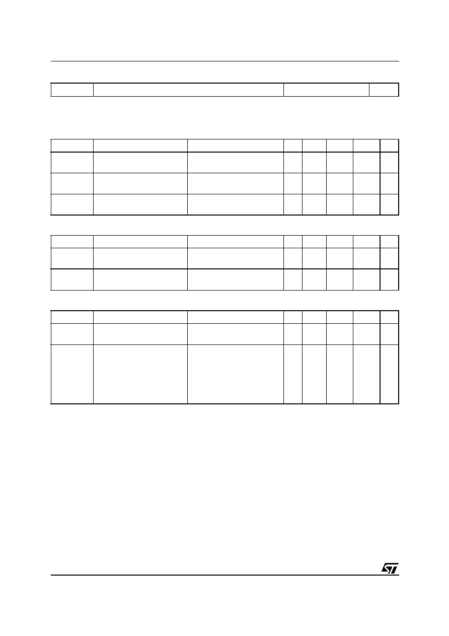
STS3C2F100
2/11
TAB.1 THERMAL DATA
(1)
when mounted on 1 in
2
pad of 2 oz. copper, t
10sec.
ELECTRICAL CHARACTERISTICS (T
j
= 25 �C unless otherwise specified)
TAB.2 OFF
TAB.3 ON
TAB.4 DYNAMIC
Rthj-amb
(1)
Thermal Resistance Junction-ambient
62.5
�C/W
Symbol
Parameter
Test Conditions
Min.
Typ.
Max.
Unit
V
(BR)DSS
Drain-source
Breakdown Voltage
I
D
= 250 �A, V
GS
= 0
n-ch
p-ch
100
V
I
DSS
Zero Gate Voltage
Drain Current (V
GS
= 0)
V
DS
= Max Rating
V
DS
= Max Rating T
C
= 125�C
n-ch
p-ch
1
10
�A
�A
I
GSS
Gate-body Leakage
Current (V
DS
= 0)
V
GS
= � 20 V
n-ch
p-ch
�100
nA
Symbol
Parameter
Test Conditions
Min.
Typ.
Max.
Unit
V
GS(th)
Gate Threshold Voltage
V
DS
= V
GS
I
D
= 250 �A
n-ch
p-ch
2
2
V
V
R
DS(on)
Static Drain-source On
Resistance
V
GS
= 10 V
I
D
= 1.5 A
V
GS
= 10 V
I
D
= 1.0 A
n-ch
p-ch
0.110
0.320
0.145
0.380
Symbol
Parameter
Test Conditions
Min.
Typ.
Max.
Unit
g
fs (*)
Forward Transconductance
V
DS
= 20 V
I
D
= 1.5 A
V
DS
= 30 V
I
D
= 1.0 A
n-ch
p-ch
3
4
S
S
C
iss
C
oss
C
rss
Input Capacitance
Output Capacitance
Reverse Transfer
Capacitance
V
DS
= 25V, f = 1 MHz, V
GS
= 0
n-ch
p-ch
n-ch
p-ch
n-ch
p-ch
460
705
70
83
30
30
pF
pF
pF
pF
pF
pF
3/11
STS3C2F100
TAB.5 SWITCHING ON
TAB.6 SWITCHING OFF
TAB.7 SOURCE DRAIN DIODE
(
)
Pulsed: Pulse duration = 300 �s, duty cycle 1.5 %.
(
�)
Pulse width limited by safe operating area.
Symbol
Parameter
Test Conditions
Min.
Typ.
Max.
Unit
t
d(on)
t
r
Turn-on Delay Time
Rise Time
N-CHANNEL
V
DD
= 50 V
I
D
= 1.5 A
R
G
= 4.7
V
GS
= 10 V
P-CHANNEL
V
DD
= 50 V
I
D
= 1.5 A
R
G
= 4.7
V
GS
= 10 V
(Resistive Load, Figure 1)
n-ch
p-ch
n-ch
p-ch
16
14
25
20
ns
ns
ns
ns
Qg
Q
gs
Q
gd
Total Gate Charge
Gate-Source Charge
Gate-Drain Charge
N-CHANNEL
V
DD
=80V I
D
=3A
V
GS
=10V
P-CHANNEL
V
DD
= 80V I
D
= 1.5A V
GS
= 10V
(see test circuit, Figure 2)
n-ch
p-ch
n-ch
p-ch
n-ch
p-ch
15
20
3.7
2.0
4.7
6.0
20
27
nC
nC
nC
nC
nC
nC
Symbol
Parameter
Test Conditions
Min.
Typ.
Max.
Unit
t
d(off)
t
f
Turn-off Delay Time
Fall Time
N-CHANNEL
V
DD
= 50 V
I
D
= 1.5 A
R
G
= 4.7
V
GS
= 10 V
P-CHANNEL
V
DD
= 50 V
I
D
= 1.5 A
R
G
= 4.7
V
GS
= 10 V
(Resistive Load, Figure 1)
n-ch
p-ch
n-ch
p-ch
32
33
20
7.5
ns
ns
ns
ns
Symbol
Parameter
Test Conditions
Min.
Typ.
Max.
Unit
I
SD
I
SDM
(
�)
Source-drain Current
Source-drain Current (pulsed)
n-ch
p-ch
n-ch
p-ch
3.0
1.5
12
6.0
A
A
A
A
V
SD
(
)
Forward On Voltage
I
SD
= 3 A
V
GS
= 0
I
SD
= 1.5 A
V
GS
= 0
n-ch
p-ch
1.2
1.2
V
V
t
rr
Q
rr
I
RRM
Reverse Recovery Time
Reverse Recovery Charge
Reverse Recovery Current
N-CHANNEL
I
SD
= 3 A
di/dt = 100A/
�
s
V
DD
= 50
V
T
j
=150
o
C
P-CHANNEL
I
SD
= 1.5 A di/dt = 100A/
�
s
V
DD
= 50
V
T
j
=150
o
C
(see test circuit, Figure 3)
n-ch
p-ch
n-ch
p-ch
n-ch
p-ch
90
65
230
175
5.0
5.4
ns
ns
nC
nC
A
A
ELECTRICAL CHARACTERISTICS (continued)
STS3C2F100
4/11
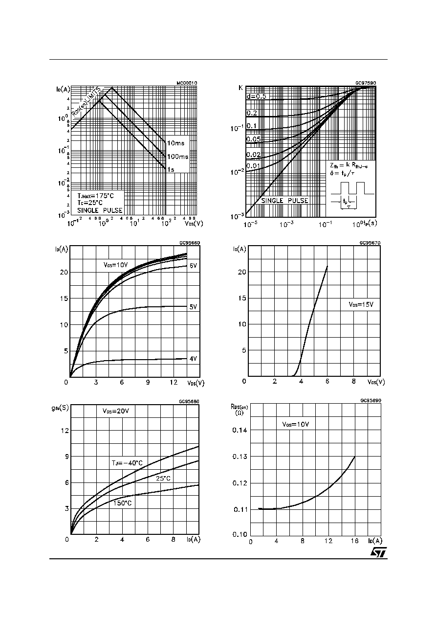
Safe Operating Area
n-ch
Thermal Impedance
n-ch
Output Characteristics
n-ch
Transfer Characteristics
n-ch
Transconductance
n-ch
Static Drain-source On Resistance
n-ch

5/11
STS3C2F100
Gate Charge vs Gate-source Voltage
n-ch
Capacitance Variations
n-ch
Normalized Gate Threshold Voltage vs Temperature
n-ch
Normalized on Resistance vs Temperature
n-ch
Source-drain Diode Forward Characteristics
n-ch
Normalized Breakdown Voltage vs Temperature
n-ch