
1/6
PRELIMINARY DATA
July 2001
STS1HNC60
N-CHANNEL 600V - 7
- 0.4A SO-8
PowerMeshTMII MOSFET
s
TYPICAL R
DS
(on) = 7
s
EXTREMELY HIGH dv/dt CAPABILITY
s
100% AVALANCHE TESTED
s
NEW HIGH VOLTAGE BENCHMARK
s
GATE CHARGE MINIMIZED
DESCRIPTION
Using the latest high voltage MESH OVERLAYTMII
process, STMicroelectronics has designed an ad-
vanced family of power MOSFETs with outstanding
performances. The new patent pending strip layout
coupled with the Company's proprietary edge termi-
nation structure, gives the lowest RDS(on) per area,
exceptional avalanche and dv/dt capabilities and
unrivalled gate charge and switching characteris-
tics.
APPLICATIONS
s
SWITCH MODE LOW POWER SUPPIES
(SMPS)
s
CFL
ABSOLUTE MAXIMUM RATINGS
(�)Pulse width limited by safe operating area
TYPE
V
DSS
R
DS(on)
I
D
STS1HNC60
600 V
< 8
0.36 A
Symbol
Parameter
Value
Unit
V
DS
Drain-source Voltage (V
GS
= 0)
600
V
V
DGR
Drain-gate Voltage (R
GS
= 20 k
)
600
V
V
GS
Gate- source Voltage
� 30
V
I
D
Drain Current (continuos) at T
C
= 25�C
0.36
A
I
D
Drain Current (continuos) at T
C
= 100�C
0.22
A
I
DM
(
q
)
Drain Current (pulsed)
1.44
A
P
TOT
Total Dissipation at T
C
= 25�C
2.5
W
Derating Factor
0.028
W/�C
dv/dt(1)
Peak Diode Recovery voltage slope
3.5
V/ns
T
stg
Storage Temperature
�65 to 150
�C
T
j
Max. Operating Junction Temperature
150
�C
(1)I
SD
0.36 A, di/dt
100A/�s, V
DD
V
(BR)DSS
, T
j
T
JMAX.
SO-8
INTERNAL SCHEMATIC DIAGRAM
STS1HNC60
2/6
THERMAL DATA
AVALANCHE CHARACTERISTICS
ELECTRICAL CHARACTERISTICS (TCASE = 25 �C UNLESS OTHERWISE SPECIFIED)
OFF
ON
(1)
DYNAMIC
Rthj-case
Rthj-amb
T
l
Thermal Resistance Junction-case
Thermal Resistance Junction-ambient Max
(Surface Mounted)
Maximum Lead Temperature For Soldering Purpose
35.7
60
300
�C/W
�C/W
�C
Symbol
Parameter
Max Value
Unit
I
AR
Avalanche Current, Repetitive or Not-Repetitive
(pulse width limited by T
j
max)
0.4
A
E
AS
Single Pulse Avalanche Energy
(starting T
j
= 25 �C, I
D
= I
AR
, V
DD
= 50 V)
100
mJ
Symbol
Parameter
Test Conditions
Min.
Typ.
Max.
Unit
V
(BR)DSS
Drain-source
Breakdown Voltage
I
D
= 250 �A, V
GS
= 0
600
V
I
DSS
Zero Gate Voltage
Drain Current (V
GS
= 0)
V
DS
= Max Rating
1
�A
V
DS
= Max Rating, T
C
= 125 �C
50
�A
I
GSS
Gate-body Leakage
Current (V
DS
= 0)
V
GS
= � 30V
�100
nA
Symbol
Parameter
Test Conditions
Min.
Typ.
Max.
Unit
V
GS(th)
Gate Threshold Voltage
V
DS
= V
GS
, I
D
= 250 �A
2
3
4
V
R
DS(on)
Static Drain-source On
Resistance
V
GS
= 10V, I
D
= 0.3 A
7
8
Symbol
Parameter
Test Conditions
Min.
Typ.
Max.
Unit
g
fs
Forward Transconductance
V
DS
> I
D(on)
x R
DS(on)max,
I
D
= 0.3 A
1.25
S
C
iss
Input Capacitance
V
DS
= 25V, f = 1 MHz, V
GS
= 0
160
pF
C
oss
Output Capacitance
26
pF
C
rss
Reverse Transfer
Capacitance
3.8
pF
3/6
STS1HNC60
ELECTRICAL CHARACTERISTICS (CONTINUED)
SWITCHING ON
SWITCHING OFF
SOURCE DRAIN DIODE
Note: 1. Pulsed: Pulse duration = 300 �s, duty cycle 1.5 %.
2. Pulse width limited by safe operating area.
Symbol
Parameter
Test Conditions
Min.
Typ.
Max.
Unit
t
d(on)
Turn-on Delay Time
Rise Time
V
DD
= 300V, I
D
= 0.7 A
R
G
= 4.7
, V
GS
= 10V
(see test circuit, Figure 3)
8
ns
t
r
8
ns
Q
g
Total Gate Charge
V
DD
= 480V, I
D
= 1.4 A,
V
GS
= 10V, R
G
= 4.7
8.5
11.5
nC
Q
gs
Gate-Source Charge
2.8
nC
Q
gd
Gate-Drain Charge
2.8
nC
Symbol
Parameter
Test Conditions
Min.
Typ.
Max.
Unit
t
r(Voff)
Off-voltage Rise Time
V
DD
= 480 V, I
D
= 1.4 A,
R
G
= 4.7
,
V
GS
= 10V
(see test circuit, Figure 5)
25
ns
t
f
Fall Time
9
ns
t
c
Cross-over Time
34
ns
Symbol
Parameter
Test Conditions
Min.
Typ.
Max.
Unit
I
SD
Source-drain Current
0.4
A
I
SDM
(2)
Source-drain Current (pulsed)
1.6
A
V
SD
(1)
Forward On Voltage
I
SD
= 0.4 A, V
GS
= 0
1.6
V
t
rr
Reverse Recovery Time
I
SD
= 1.4 A, di/dt = 100A/�s,
V
DD
= 100V, T
j
= 150�C
(see test circuit, Figure 5)
500
ns
Q
rr
Reverse Recovery Charge
950
�
C
I
RRM
Reverse Recovery Current
3.8
A

STS1HNC60
4/6
Fig. 5: Test Circuit For Inductive Load Switching
And Diode Recovery Times
Fig. 4: Gate Charge test Circuit
Fig. 2: Unclamped Inductive Waveform
Fig. 1: Unclamped Inductive Load Test Circuit
Fig. 3: Switching Times Test Circuit For
Resistive Load
5/6
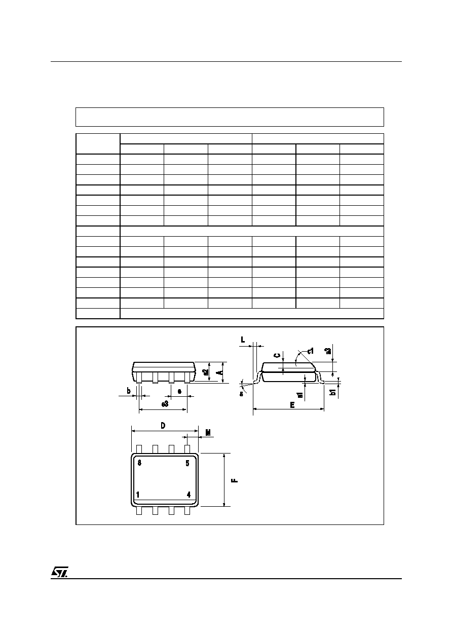
STS1HNC60
DIM.
mm
inch
MIN.
TYP.
MAX.
MIN.
TYP.
MAX.
A
1.75
0.068
a1
0.1
0.25
0.003
0.009
a2
1.65
0.064
a3
0.65
0.85
0.025
0.033
b
0.35
0.48
0.013
0.018
b1
0.19
0.25
0.007
0.010
C
0.25
0.5
0.010
0.019
c1
45 (typ.)
D
4.8
5.0
0.188
0.196
E
5.8
6.2
0.228
0.244
e
1.27
0.050
e3
3.81
0.150
F
3.8
4.0
0.14
0.157
L
0.4
1.27
0.015
0.050
M
0.6
0.023
S
8 (max.)
0016023
SO-8 MECHANICAL DATA