1/5
STPS1045B/H
®
July 2003 - Ed: 3B
POWER SCHOTTKY RECTIFIER
I
F(AV)
10 A
V
RRM
45 V
V
F
(max)
0.57 V
MAIN PRODUCT CHARACTERISTICS
n
NEGLIGIBLE SWITCHING LOSSES
n
LOW FORWARD DROP VOLTAGE
n
LOW CAPACITANCE
n
HIGH REVERSE AVALANCHE SURGE
CAPABILITY
n
AVALANCHE CAPABILITY SPECIFIED
FEATURES AND BENEFITS
High voltage Schottky rectifier suited for Switch
Mode
Power
Supplies
and
other
Power
Converters.
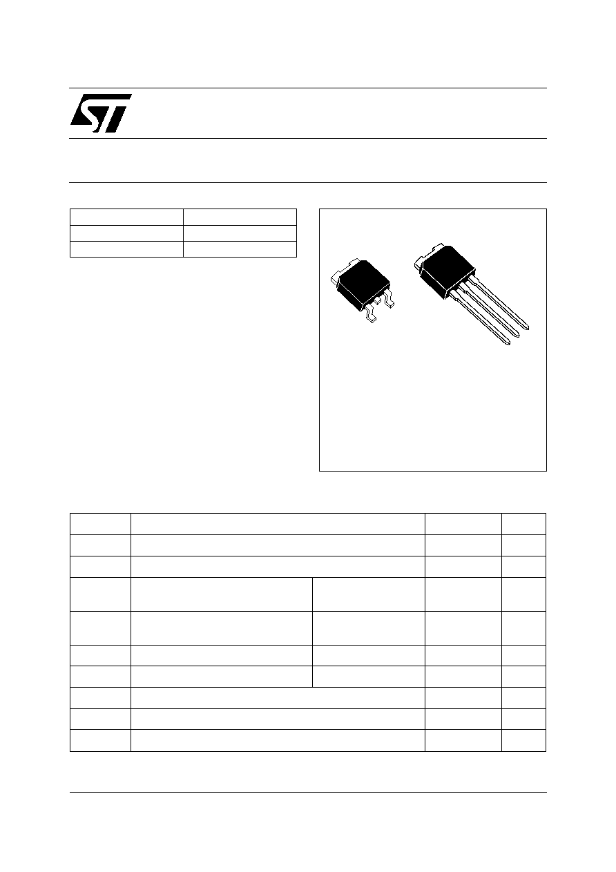
Packaged in DPAK and IPAK, these devices are
intended for use
in high frequency circuitries
where low switching losses are required.
DESCRIPTION
DPAK
STPS1045B
A
A
K
K
A
A
K
K
Symbol
Parameter
Value
Unit
V
RRM
Repetitive peak reverse voltage
45
V
I
F(RMS)
/ pin
RMS forward current / pin
7
A
I
F(AV)
Average forward current
Tc = 150°C
d = 0.5
10
A
I
FSM
Surge non repetitive forward current
tp = 10 ms
Sinusoidal
75
A
I
RRM
Repetitive peak reverse current
tp = 2 µs F = 1KHz
1
A
P
ARM
Repetitive peak avalanche power
tp = 1µs
Tj = 25°C
4000
W
T
stg
Storage temperature range
- 65 to + 175
°C
Tj
Maximum junction temperature
175
°C
dV/dt
Critical rate of rise of reverse voltage
10000
V/µs
ABSOLUTE MAXIMUM RATINGS
IPAK
STPS1045H

STPS1045B/H
2/5
Symbol
Parameter
Value
Unit
R
th (j-c)
Junction to case
3
°C/W
THERMAL RESISTANCES
Symbol
Parameter
Tests Conditions
Min.
Typ.
Max.
Unit
I
R
*
Reverse leakage current
Tj = 25°C
V
R
= 45 V
100
µ
A
Tj = 125°C
7
15
mA
V
F
**
Forward voltage drop
Tj = 25°C
I
F
= 10 A
0.63
V
Tj = 125°C
I
F
= 10 A
0.5
0.57
Tj = 25°C
I
F
= 20 A
0.84
Tj = 125°C
I
F
= 20 A
0.65
0.72
STATIC ELECTRICAL CHARACTERISTICS
Pulse test :
* tp = 380 µs,
< 2 %
**tp = 5 ms,
< 2%
To evaluate the maximum conduction losses use the following equation :
P = 0.42 x I
F(AV)
+ 0.015 I
F
2
(RMS)
0
1
2
3
4
5
6
7
8
9
10
11
12
0
1
2
3
4
5
6
7
8
IF(av) (A)
PF(av)(W)
= 0.05
= 0.1
= 0.2
= 0.5
= 1
T
=tp/T
tp
Fig. 1: Average forward power dissipation versus
average forward current.
0
25
50
75
100
125
150
175
0
2
4
6
8
10
12
Tamb(°C)
IF(av)(A)
Rth(j-a)=15°C/W
Rth(j-a)=Rth(j-c)
Rth(j-a)=70°C/W
T
=tp/T
tp
Fig. 2: Average forward current versus ambient
temperature (
=0.5).
0
0.2
0.4
0.6
0.8
1
1.2
0
25
50
75
100
125
150
T (°C)
j
P
(t )
P
(25°C)
ARM p
ARM
Fig. 4: Normalized avalanche power derating
versus junction temperature.
0.001
0.01
0.1
0.01
1
0.1
10
100
1000
1
t (µs)
p
P
(t )
P
(1µs)
ARM p
ARM
Fig. 3: Normalized avalanche power derating
versus pulse duration.

STPS1045B/H
3/5
0
5
10
15
20
25
30
35
40
45
1E-1
1E+0
1E+1
1E+2
1E+3
1E+4
1E+5
VR(V)
IR(µA)
Tj=150°C
Tj=100°C
Tj=125°C
Tj=25°C
Tj=50°C
Tj=75°C
Fig. 7: Reverse leakage current versus reverse
voltage applied (typical values).
0.0
0.2
0.4
0.6
0.8
1.0
1.2
1.4
1.6
0.1
1.0
10.0
100.0
VFM(V)
IFM(A)
Tj=125°C
Tj=25°C
Tj=125°C
(Typical values)
Fig. 9: Forward voltage drop versus forward
current (maximum values).
1
2
5
10
20
50
100
200
500
1000
VR(V)
C(pF)
F=1MHz
Tj=25°C
Fig. 8: Junction capacitance versus reverse
voltage applied (typical values).
0
2
4
6
8
10
12
14
16
18
20
0
20
40
60
80
100
S(Cu) (cm˛)
Rth(j-a) (°C/W)
Fig. 10: Thermal resistance junction to ambient
versus copper surface under tab (Epoxy printed
circuit
board,
copper
thickness:
35µm
)
(
STPS1045B)
.
1E-3
1E-2
1E-1
1E+0
0
20
40
60
80
100
120
t(s)
IM(A)
Tc=50°C
Tc=100°C
Tc=150°C
I
M
t
=0.5
Fig. 5: Non repetitive surge peak forward current
versus overload duration (maximum values).
1E-4
1E-3
1E-2
1E-1
1E+0
0.0
0.2
0.4
0.6
0.8
1.0
tp(s)
Zth(j-c)/Rth(j-c)
T
=tp/T
tp
Single pulse
= 0.1
= 0.2
= 0.5
Fig. 6: Relative variation of thermal impedance
junction to case versus pulse duration.
STPS1045B/H
4/5
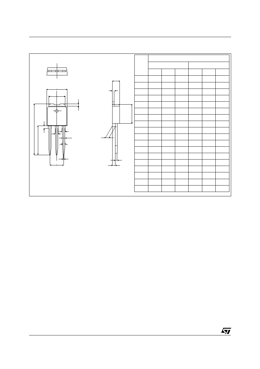
PACKAGE MECHANICAL DATA
IPAK
H
L
L1
G
B5
B
V1
D
C
A1
A3
A
C2
B3
B6
L2
E
B2
REF.
DIMENSIONS
Millimeters
Inches
Min.
Typ.
Max.
Min.
Typ.
Max.
A
2.2
2.4
0.086
0.094
A1
0.9
1.1
0.035
0.043
A3
0.7
1.3
0.027
0.051
B
0.64
0.9
0.025
0.035
B2
5.2
5.4
0.204
0.212
B3
0.85
0.033
B5
0.3
0.035
B6
0.95
0.037
C
0.45
0.6
0.017
0.023
C2
0.48
0.6
0.019
0.023
D
6
6.2
0.236
0.244
E
6.4
6.6
0.252
0.260
G
4.4
4.6
0.173
0.181
H
15.9
16.3 0.626
0.641
L
9
9.4
0.354
0.370
L1
0.8
1.2
0.031
0.047
L2
0.8
1
0.031 0.039
V1
10°
10°
n
COOLING METHOD: BY CONDUCTION (C)
STPS1045B/H
5/5
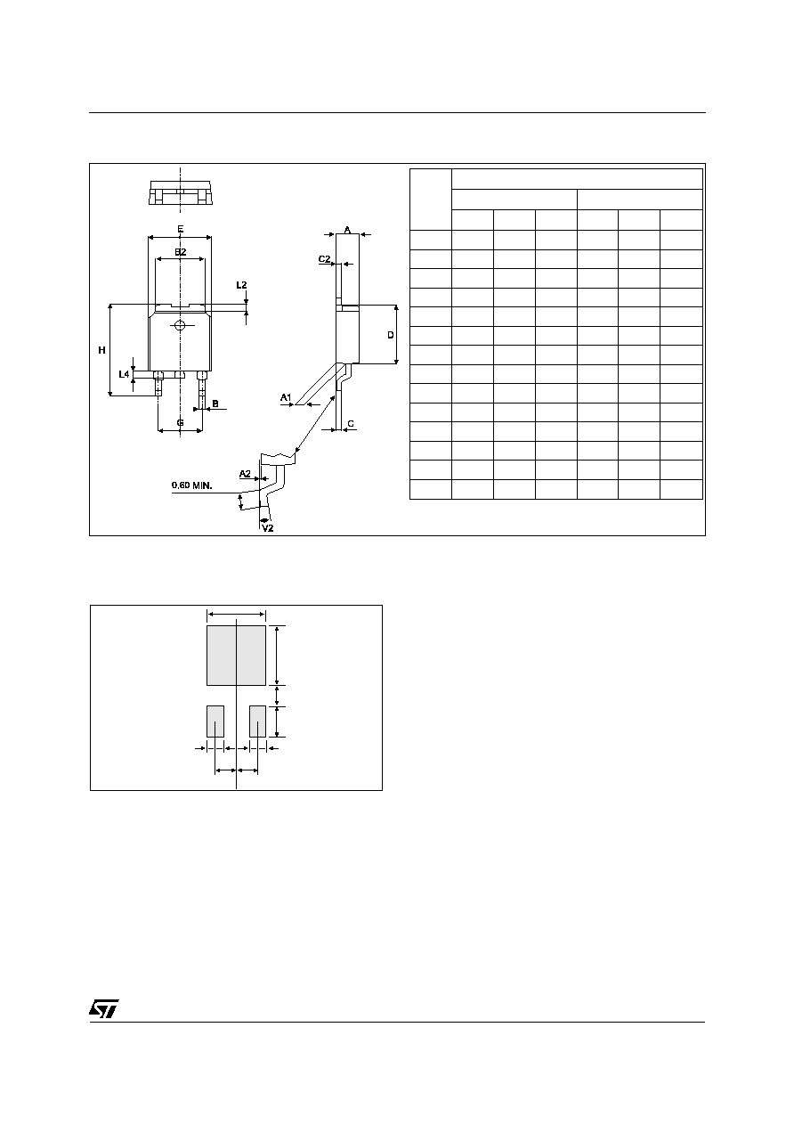
REF.
DIMENSIONS
Millimeters
Inches
Min.
Typ.
Max
Min.
Typ.
Max.
A
2.20
2.40 0.086
0.094
A1
0.90
1.10 0.035
0.043
A2
0.03
0.23 0.001
0.009
B
0.64
0.90 0.025
0.035
B2
5.20
5.40 0.204
0.212
C
0.45
0.60 0.017
0.023
C2
0.48
0.60 0.018
0.023
D
6.00
6.20 0.236
0.244
E
6.40
6.60 0.251
0.259
G
4.40
4.60 0.173
0.181
H
9.35
10.10 0.368
0.397
L2
0.80
0.031
L4
0.60
1.00 0.023
0.039
V2
0°
8°
0°
8°
PACKAGE MECHANICAL DATA
DPAK
Information furnished is believed to be accurate and reliable. However, STMicroelectronics assumes no responsibility for the consequences of
use of such information nor for any infringement of patents or other rights of third parties which may result from its use. No license is granted by
implication or otherwise under any patent or patent rights of STMicroelectronics. Specifications mentioned in this publication are subject to
change without notice. This publication supersedes and replaces all information previously supplied.
STMicroelectronics products are not authorized for use as critical components in life support devices or systems without express written
approval of STMicroelectronics.
The ST logo is a registered trademark of STMicroelectronics
© 2003 STMicroelectronics - Printed in Italy - All rights reserved.
STMicroelectronics GROUP OF COMPANIES
Australia - Brazil - Canada - China - Finland - France - Germany
Hong Kong - India - Israel - Italy - Japan - Malaysia - Malta - Morocco - Singapore
Spain - Sweden - Switzerland - United Kingdom - United States.
6.7
6.7
6.7
3
1.6
1.6
2.3
2.3
FOOT PRINT DIMENSIONS (in millimeters)
n
COOLING METHOD: BY CONDUCTION (C)