STP6NA60FP
N - CHANNEL ENHANCEMENT MODE
FAST POWER MOS TRANSISTOR
PRELIMINARY DATA
s
TYPICAL R
DS(on)
= 1
s
ḟ
30V GATE TO SOURCE VOLTAGE RATING
s
100% AVALANCHE TESTED
s
REPETITIVE AVALANCHE DATA AT 100
o
C
s
LOW INTRINSIC CAPACITANCES
s
GATE CHARGE MINIMIZED
s
REDUCED THRESHOLD VOLTAGE SPREAD
DESCRIPTION
This series of POWER MOSFETS represents
the most advanced high voltage technology.
The optmized cell layout coupled with a new
proprietary edge termination concur to give
the device low
RDS(on) and gate charge,
unequalled
ruggedness
and
superior
switching performance.
APPLICATIONS
s
HIGH CURRENT, HIGH SPEED SWITCHING
s
SWITCH MODE POWER SUPPLIES (SMPS)
s
DC-AC CONVERTERS FOR WELDING
EQUIPMENT AND UNINTERRUPTIBLE
POWER SUPPLIES AND MOTOR DRIVE
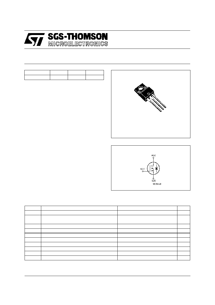
INTERNAL SCHEMATIC DIAGRAM
ABSOLUTE MAXIMUM RATINGS
Symbol
Parameter
Valu e
Unit
V
DS
Drain-source Voltage (V
GS
= 0)
600
V
V
DGR
Drain- gate Voltage (R
G S
= 20 k
)
600
V
V
GS
Gate-source Voltage
ḟ
30
V
I
D
Drain Current (cont inuous) at T
c
= 25
o
C
3.9
A
I
D
Drain Current (cont inuous) at T
c
= 100
o
C
2.6
A
I
DM
(
Ṗ
)
Drain Current (pulsed)
26
A
P
t ot
Tot al Dissipation at T
c
= 25
o
C
40
W
Derating Fact or
0.32
W/
o
C
V
ISO
Insulation W it hstand Voltage (DC)
2000
V
T
stg
St orage Temperature
-65 to 150
o
C
T
j
Max. Operat ing Junction Temperat ure
150
o
C
(
Ṗ
) Pulse width limited by safe operating area
TYPE
V
DSS
R
DS(on)
I
D
STP6NA60F P
600 V
< 1.2
3.9 A
October 1997
1
2
3
TO-220FP
1/5

THERMAL DATA
R
t hj-ca se
R
t hj- amb
R
thc- si nk
T
l
Thermal Resistance Junction-case
Max
Thermal Resistance Junction-ambient
Max
Thermal Resistance Case-sink
Typ
Maximum Lead Temperature For Soldering Purpose
3. 12
62. 5
0.5
300
o
C/ W
oC/W
o
C/ W
o
C
AVALANCHE CHARACTERISTICS
Symb ol
Parameter
Max Valu e
Uni t
I
AR
Avalanche Current, Repetitive or Not -Repet itive
(pulse width limited by T
j
max,
< 1%)
6.5
A
E
AS
Single Pulse Avalanche Energy
(starting T
j
= 25
o
C, I
D
= I
AR
, V
DD
= 50 V)
215
mJ
ELECTRICAL CHARACTERISTICS (T
case
= 25
o
C unless otherwise specified)
OFF
Symb ol
Parameter
Test Cond ition s
Mi n.
Typ .
Max.
Un it
V
(BR)DSS
Drain-source
Breakdown Volt age
I
D
= 250
ṁ
A
V
GS
= 0
600
V
I
DSS
Zero
Gate
Voltage
Drain Current (V
GS
= 0)
V
DS
= Max Rating
V
DS
= Max Rating
T
c
= 100
o
C
25
250
ṁ
A
ṁ
A
I
GSS
Gate-body
Leakage
Current (V
DS
= 0)
V
G S
=
ḟ
30 V
ḟ
100
nA
ON (
)
Symb ol
Parameter
Test Cond ition s
Mi n.
Typ .
Max.
Un it
V
GS(th)
Gate
Threshold
Voltage
V
DS
= V
GS
I
D
= 250
ṁ
A
2.25
3
3.75
V
R
DS( on)
St atic Drain-source On
Resistance
V
G S
= 10V I
D
= 2.5 A
1
1.2
I
D(o n)
On St ate Drain Current
V
DS
> I
D(on)
x R
DS(on) max
V
G S
= 10 V
6. 5
A
DYNAMIC
Symb ol
Parameter
Test Cond ition s
Mi n.
Typ .
Max.
Un it
g
fs
(
)
Forward
Transconduct ance
V
DS
> I
D(on)
x R
DS(on) max
I
D
= 3 A
3. 5
5.6
S
C
iss
C
oss
C
rss
Input Capacitance
Output Capacit ance
ReverseTransfer
Capacitance
V
DS
= 25 V
f = 1 MHz
V
GS
= 0
1150
155
40
1550
210
55
pF
pF
pF
STP6NA60FP
2/5

ELECTRICAL CHARACTERISTICS (continued)
SWITCHING ON
Symb ol
Parameter
Test Cond ition s
Mi n.
Typ .
Max.
Un it
t
d(on)
t
r
Turn-on Time
Rise Time
V
DD
= 300
V
I
D
=
3
A
R
G
= 47
V
G S
= 10 V
35
90
55
125
ns
ns
Q
g
Q
gs
Q
gd
Total Gate Charge
Gate-Source Charge
Gate-Drain Charge
V
DD
= 480 V
I
D
= 3 A
V
GS
= 10 V
54
8
23
75
nC
nC
nC
SWITCHING OFF
Symb ol
Parameter
Test Cond ition s
Mi n.
Typ .
Max.
Un it
t
r(Vof f)
t
f
t
c
Of f-voltage Rise Time
Fall Time
Cross-over Time
V
DD
= 480 V
I
D
= 6 A
R
G
= 47
V
GS
= 10 V
(see test circuit, figure 5)
80
20
115
110
30
155
ns
ns
ns
SOURCE DRAIN DIODE
Symb ol
Parameter
Test Cond ition s
Mi n.
Typ .
Max.
Un it
I
SD
I
SDM
(
Ṗ
)
Source-drain Current
Source-drain
Current
(pulsed)
6.5
26
A
A
V
SD
(
)
Forward On Voltage
I
SD
= 6. 5 A
V
GS
= 0
1.6
V
t
rr
Q
rr
I
RRM
Reverse
Recovery
Time
Reverse
Recovery
Charge
Reverse
Recovery
Current
I
SD
= 6 A
di/dt = 100 A/
ṁ
s
V
DD
= 100 V
T
j
= 150
o
C
(see circuit, figure 5)
600
9
30
ns
ṁ
C
A
(
) Pulsed: Pulse duration = 300
ṁ
s, duty cycle 1.5 %
(
Ṗ
) Pulse width limited by safe operating area
STP6NA60FP
3/5
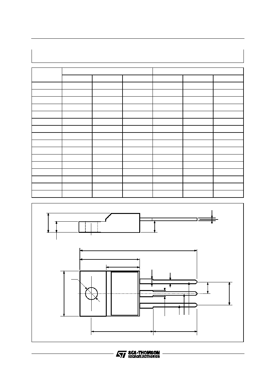
DIM.
mm
inch
MIN.
TYP.
MAX.
MIN.
TYP.
MAX.
A
4.4
4.6
0.173
0.181
B
2.5
2.7
0.098
0.106
D
2.5
2.75
0.098
0.108
E
0.45
0.7
0.017
0.027
F
0.75
1
0.030
0.039
F1
1.15
1.7
0.045
0.067
F2
1.15
1.7
0.045
0.067
G
4.95
5.2
0.195
0.204
G1
2.4
2.7
0.094
0.106
H
10
10.4
0.393
0.409
L2
16
0.630
L3
28.6
30.6
1.126
1.204
L4
9.8
10.6
0.385
0.417
L6
15.9
16.4
0.626
0.645
L7
9
9.3
0.354
0.366
Ø
3
3.2
0.118
0.126
L2
A
B
D
E
H
G
L6
Ÿ
F
L3
G1
1 2 3
F2
F1
L7
L4
TO-220FP MECHANICAL DATA
STP6NA60FP
4/5

Information furnished is believed to be accurate and reliable. However, SGS-THOMSON Microelectronics assumes no responsability for the
consequences of use of such information nor for any infringement of patents or other rights of third parties which may results from its use. No
license is granted by implication or otherwise under any patent or patent rights of SGS-THOMSON Microelectronics. Specifications mentioned
in this publication are subject to change without notice. This publication supersedes and replaces all information previously supplied.
SGS-THOMSON Microelectronics products are not authorized for use as critical components in life support devices or systems without express
written approval of SGS-THOMSON Microelectonics.
©
1997 SGS-THOMSON Microelectronics - Printed in Italy - All Rights Reserved
SGS-THOMSON Microelectronics GROUP OF COMPANIES
Australia - Brazil - Canada - China - France - Germany - Hong Kong - Italy - Japan - Korea - Malaysia - Malta - Morocco - The Netherlands -
Singapore - Spain - Sweden - Switzerland - Taiwan - Thailand - United Kingdom - U.S.A
. . .
STP6NA60FP
5/5