1/9
April 2002
STP5NK65Z
N-CHANNEL 650V - 1.5
- 5A TO-220
Zener-Protected SuperMESHTMPower MOSFET
s
TYPICAL R
DS
(on) = 1.5
s
EXTREMELY HIGH dv/dt CAPABILITY
s
IMPROVED ESD CAPABILITY
s
100% AVALANCHE RATED
s
GATE CHARGE MINIMIZED
s
VERY LOW INTRINSIC CAPACITANCES
s
VERY GOOD MANUFACTURING
REPEATIBILITY
DESCRIPTION
The SuperMESHTM series is obtained through an
extreme optimization of ST's well established strip-
based PowerMESHTM layout. In addition to pushing
on-resistance significantly down, special care is tak-
en to ensure a very good dv/dt capability for the
most demanding applications. Such series comple-
ments ST full range of high voltage MOSFETs in-
cluding revolutionary MDmeshTM products.
APPLICATIONS
s
HIGH CURRENT, HIGH SPEED SWITCHING
s
IDEAL FOR OFF-LINE POWER SUPPLIES,
ADAPTORS AND PFC
ORDERING INFORMATION
TYPE
V
DSS
R
DS(on)
I
D
Pw
STP5NK65Z
650 V
< 1.8
5 A
85 W
SALES TYPE
MARKING
PACKAGE
PACKAGING
STP5NK65Z
P5NK65Z
TO-220
TUBE
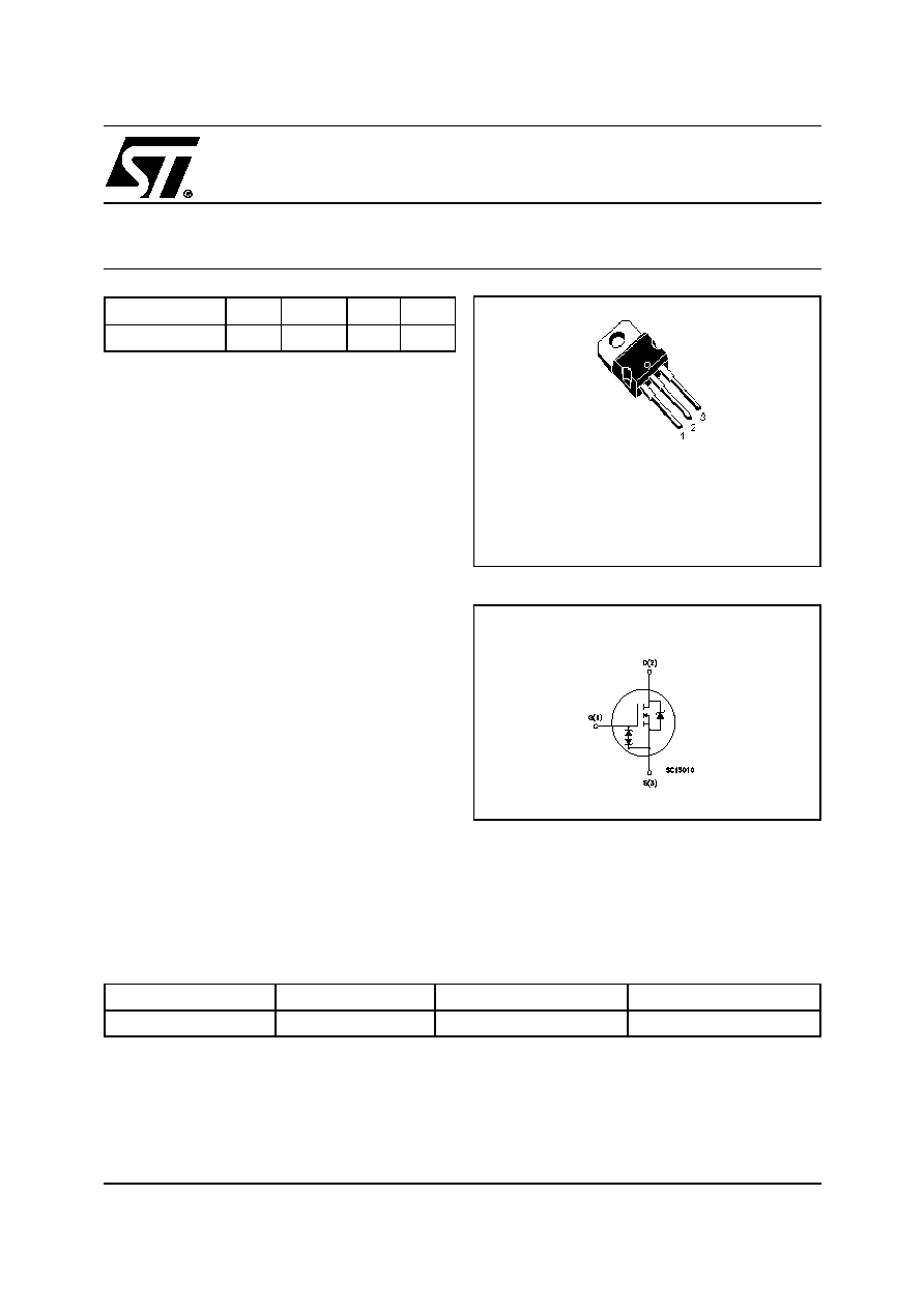
TO-220
INTERNAL SCHEMATIC DIAGRAM
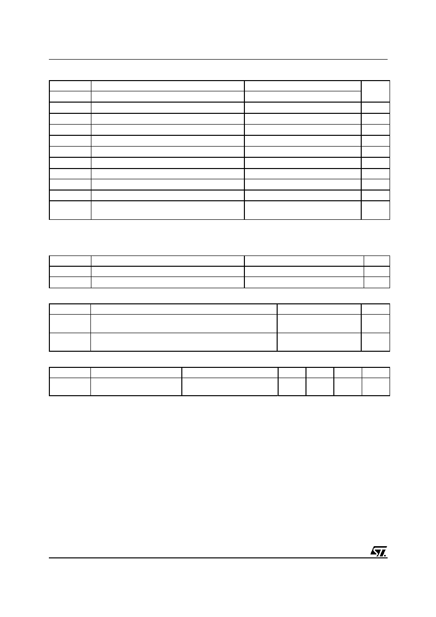
STP5NK65Z
2/9
ABSOLUTE MAXIMUM RATINGS
(
l
) Pulse width limited by safe operating area
(1) I
SD
5A, di/dt
100
µ
A, V
DD
V
(BR)DSS
, T
j
T
JMAX.
(*) Limited only by maximum temperature allowed
THERMAL DATA
AVALANCHE CHARACTERISTICS
GATE-SOURCE ZENER DIODE
PROTECTION FEATURES OF GATE-TO-SOURCE ZENER DIODES
The built-in back-to-back Zener diodes have specifically been designed to enhance not only the device's
ESD capability, but also to make them safely absorb possible voltage transients that may occasionally be
applied from gate to souce. In this respect the Zener voltage is appropriate to achieve an efficient and cost-
effective intervention to protect the device's integrity. These integrated Zener diodes thus avoid the usage
of external components.
Symbol
Parameter
Value
Unit
V
DS
Drain-source Voltage (V
GS
= 0)
650
V
V
DGR
Drain-gate Voltage (R
GS
= 20 k
)
650
V
V
GS
Gate- source Voltage
± 30
V
I
D
Drain Current (continuous) at T
C
= 25°C
5
A
I
D
Drain Current (continuous) at T
C
= 100°C
3.1
A
I
DM
(
l
)
Drain Current (pulsed)
20
A
P
TOT
Total Dissipation at T
C
= 25°C
85
W
Derating Factor
0.6
W/°C
V
ESD(G-S)
Gate source ESD(HBM-C=100pF, R=1.5K
)
2000
V
dv/dt (1)
Peak Diode Recovery voltage slope
4.5
V/ns
T
j
T
stg
Operating Junction Temperature
Storage Temperature
-55 to 150
-55 to 150
°C
°C
Rthj-case
Thermal Resistance Junction-case Max
1.64
°C/W
Rthj-amb
Thermal Resistance Junction-ambient Max
50
°C/W
T
l
Maximum Lead Temperature For Soldering Purpose
300
°C
Symbol
Parameter
Max Value
Unit
I
AR
Avalanche Current, Repetitive or Not-Repetitive
(pulse width limited by T
j
max)
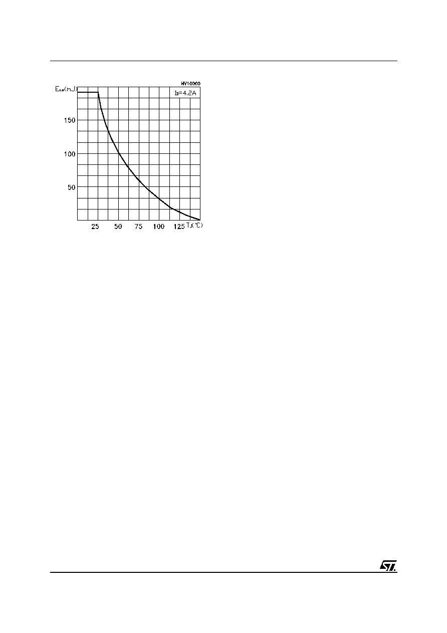
4.2
A
E
AS
Single Pulse Avalanche Energy
(starting T
j
= 25 °C, I
D
= I
AR
, V
DD
= 50 V)
190
mJ
Symbol
Parameter
Test Conditions
Min.
Typ.
Max.
Unit
BV
GSO
Gate-Source Breakdown
Voltage
Igs=± 1mA (Open Drain)
30
V
3/9
STP5NK65Z
ELECTRICAL CHARACTERISTICS (TCASE =25°C UNLESS OTHERWISE SPECIFIED)
ON/OFF
DYNAMIC
SWITCHING ON
SWITCHING OFF
SOURCE DRAIN DIODE
Note: 1. Pulsed: Pulse duration = 300 µs, duty cycle 1.5 %.
2. Pulse width limited by safe operating area.
3. C
oss eq.
is defined as a constant equivalent capacitance giving the same charging time as C
oss
when V
DS
increases from 0 to 80%
V
DSS
.
Symbol
Parameter
Test Conditions
Min.
Typ.
Max.
Unit
V
(BR)DSS
Drain-source
Breakdown Voltage
I
D
= 1 mA, V
GS
= 0
650
V
I
DSS
Zero Gate Voltage
Drain Current (V
GS
= 0)
V
DS
= Max Rating
V
DS
= Max Rating, T
C
= 125 °C
1
50
µA
µA
I
GSS
Gate-body Leakage
Current (V
DS
= 0)
V
GS
= ± 20V
±10
µA
V
GS(th)
Gate Threshold Voltage
V
DS
= V
GS
, I
D
= 50µA
3
3.75
4.5
V
R
DS(on)
Static Drain-source On
Resistance
V
GS
= 10V, I
D
= 2.1 A
1.5
1.8
Symbol
Parameter
Test Conditions
Min.
Typ.
Max.
Unit
g
fs
(1)
Forward Transconductance
V
DS
= 10 V
,
I
D
= 2.1 A
5
S
C
iss
C
oss
C
rss
Input Capacitance
Output Capacitance
Reverse Transfer
Capacitance
V
DS
= 25V, f = 1 MHz, V
GS
= 0
680
80
17
pF
pF
pF
C
oss eq.
(3)
Equivalent Output
Capacitance
V
GS
= 0V, V
DS
= 0V to 480 V
98
pF
Symbol
Parameter
Test Conditions
Min.
Typ.
Max.
Unit
t
d(on)
t
r
Turn-on Delay Time
Rise Time
V
DD
= 325 V, I
D
= 2.1 A
R
G
= 4.7
V
GS
= 10 V
(Resistive Load see, Figure 3)
20
15
ns
ns
Q
g
Q
gs
Q
gd
Total Gate Charge
Gate-Source Charge
Gate-Drain Charge
V
DD
= 520V, I
D
= 4.2 A,
V
GS
= 10V
25
4.4
13.7
35
nC
nC
nC
Symbol
Parameter
Test Conditions
Min.
Typ.
Max.
Unit
t
d(off)
t
f
Turn-off Delay Time
Fall Time
V
DD
= 325 V, I
D
= 2.1 A
R
G
= 4.7
V
GS
= 10 V
(Resistive Load see, Figure 3)
140
40
ns
ns
t
r(Voff)
t
f
t
c
Off-voltage Rise Time
Fall Time
Cross-over Time
V
DD
= 520 V, I
D
= 4.2 A,
R
G
= 4.7
,
V
GS
= 10V
(Inductive Load see, Figure 5)
12
7
15
ns
ns
ns
Symbol
Parameter
Test Conditions
Min.
Typ.
Max.
Unit
I
SD
I
SDM
(2)
Source-drain Current
Source-drain Current (pulsed)
5
20
A
A
V
SD
(1)
Forward On Voltage
I
SD
= 5 A, V
GS
= 0
1.6
V
t
rr
Q
rr
I
RRM
Reverse Recovery Time
Reverse Recovery Charge
Reverse Recovery Current
I
SD
= 4.2 A, di/dt = 100A/µs
V
DD
= 100V, T
j
= 150°C
(see test circuit, Figure 5)
375
1.76
10
ns
µC
A
STP5NK65Z
4/9
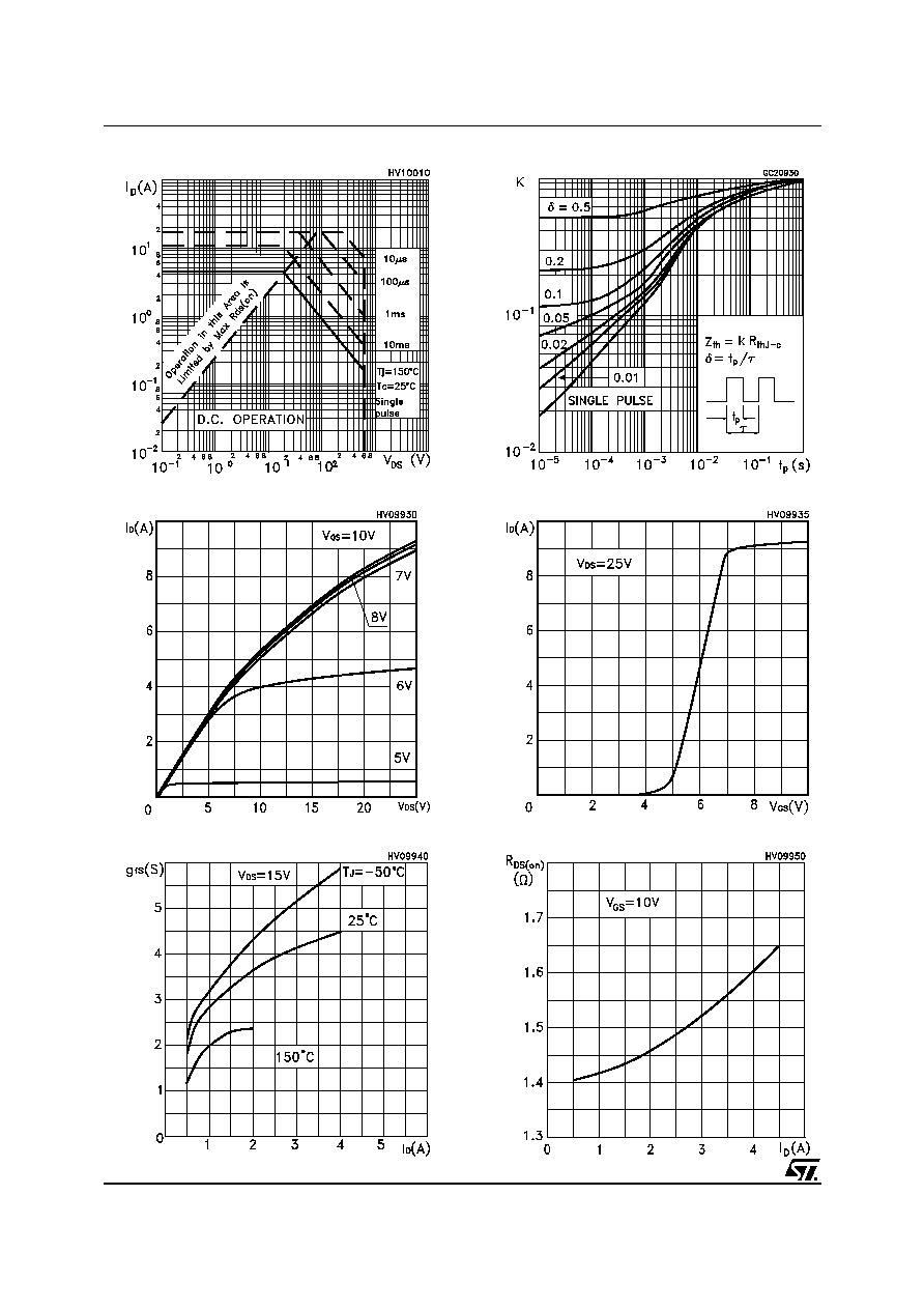
Safe Operating Area
Thermal Impedance
Transconductance
Static Drain-source On Resistance
Transfer Characteristics
Output Characteristics

5/9
STP5NK65Z
Gate Charge vs Gate-source Voltage
Capacitance Variations
Normalized On Resistance vs Temperature
Normalized BVDSS vs Temperature
Normalized Gate Threshold Voltage vs Temp.
Source-drain Diode Forward Characteristics
STP5NK65Z
6/9
Maximum Avalanche Energy vs Temperature
7/9
STP5NK65Z
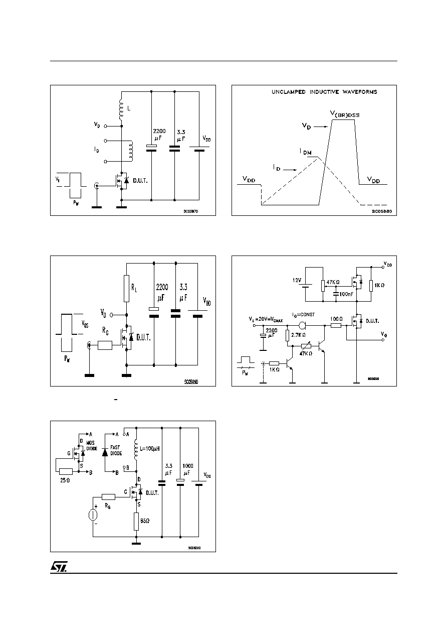
Fig. 5: Test Circuit For Inductive Load Switching
And Diode Recovery Times
Fig. 4: Gate Charge test Circuit
Fig. 2: Unclamped Inductive Waveform
Fig. 1: Unclamped Inductive Load Test Circuit
Fig. 3: Switching Times Test Circuit For
Resistive Load
STP5NK65Z
8/9
DIM.
mm
inch
MIN.
TYP.
MAX.
MIN.
TYP.
MAX.
A
4.40
4.60
0.173
0.181
C
1.23
1.32
0.048
0.051
D
2.40
2.72
0.094
0.107
D1
1.27
0.050
E
0.49
0.70
0.019
0.027
F
0.61
0.88
0.024
0.034
F1
1.14
1.70
0.044
0.067
F2
1.14
1.70
0.044
0.067
G
4.95
5.15
0.194
0.203
G1
2.4
2.7
0.094
0.106
H2
10.0
10.40
0.393
0.409
L2
16.4
0.645
L4
13.0
14.0
0.511
0.551
L5
2.65
2.95
0.104
0.116
L6
15.25
15.75
0.600
0.620
L7
6.2
6.6
0.244
0.260
L9
3.5
3.93
0.137
0.154
DIA.
3.75
3.85
0.147
0.151
L6
A
C
D
E
D1
F
G
L7
L2
Dia.
F1
L5
L4
H2
L9
F2
G1
TO-220 MECHANICAL DATA
P011C

9/9
STP5NK65Z
Information furnished is believed to be accurate and reliable. However, STMicroelectronics assumes no responsibility for the
consequences of use of such information nor for any infringement of patents or other rights of third parties which may result from
its use. No license is granted by implication or otherwise under any patent or patent rights of STMicroelectronics. Specifications
mentioned in this publication are subject to change without notice. This publication supersedes and replaces all information
previously supplied. STMicroelectronics products are not authorized for use as critical components in life support devices or
systems without express written approval of STMicroelectronics.
© The ST logo is a registered trademark of STMicroelectronics
© 2002 STMicroelectronics - Printed in Italy - All Rights Reserved
STMicroelectronics GROUP OF COMPANIES
Australia - Brazil - Canada - China - Finland - France - Germany - Hong Kong - India - Israel - Italy - Japan - Malaysia - Malta - Morocco
Singapore - Spain - Sweden - Switzerland - United Kingdom - United States.
© http://www.st.com