1/16
October 2003
s
LOW VOLTAGE POWER SUPPLY DOWN TO
3V
s
16 CONSTANT CURRENT OUTPUT
CHANNELS
s
ADJUSTABLE OUTPUT CURRENT
THROUGH EXTERNAL RESISTOR
s
SERIAL DATA IN/PARALLEL DATA OUT
s
SERIAL OUT CHANGES STATE ON THE
FAILING EDGES OF CLOCK
s
3.3V MICRO DRIVER-ABLE
s
OUTPUT CURRENT: 5-90 mA
s
25 MHz CLOCK FREQ.
s
AVAILABLE IN HIGH THERMAL EFFICIENCY
TSSOP EXPOSED PAD
DESCRIPTION
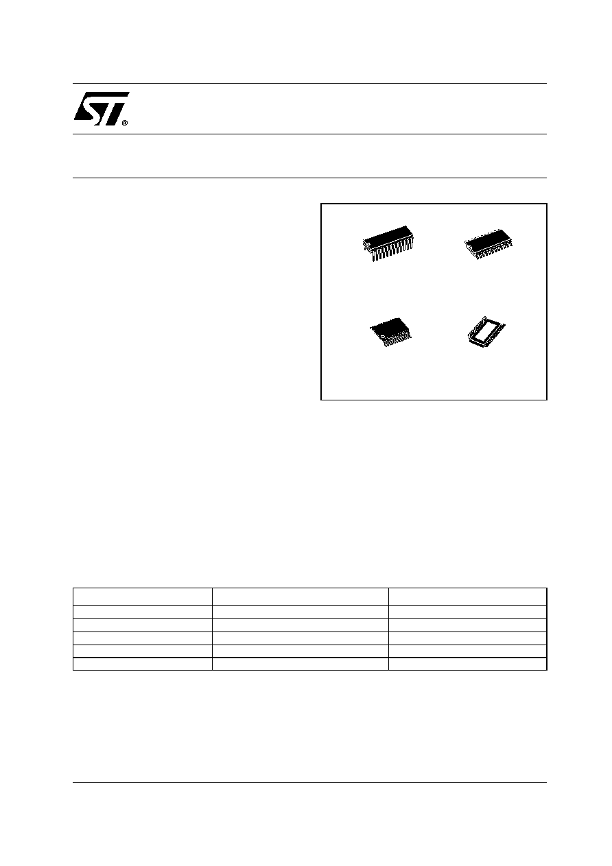
The STP16CL596 is a monolithic, low voltage, low
current power 16-bit shift register designed for
LED panel displays. The STP16CL596 contains a
16-bit serial-in, parallel-out shift register that feeds
a 16-bitD-type storage register. In the output
stage, sixteen regulated current sources were
designed to provide 5-90mA constant current to
drive the LEDs.
Compared with the STPIC6C595, the device
provides
great
flexibility
and
improved
performance in LED panel system design.
Trough an external resistor, users can adjust the
STP16CL596 output current, controlling in this
way the light intensity of LEDs.
The STP16CL596 guarantees a 16V output
driving capability, allowing users to connect more
LEDs in series. The high clock frequency, 25 MHz,
also satisfies the system requirement of high
volume data transmission. The 3.3V of voltage
supply is well useful for applications that interface
any micro from 3.3V. Compared with a standard
TSSOP package, the TSSOP exposed pad
increases heat dissipation capability by a 2.5
factor.
ORDERING CODES
Type
Package
Comments
STP16CL596B1R
DIP-24
15 parts per tube
STP16CL596M
SO-24 (Tube)
40 parts per tube
STP16CL596MR
SO-24 (Tape & Reel)
1000 parts per reel
STP16CL596TTR
TSSOP24 (Tape & Reel)
2500 parts per reel
STP16CL596XTTR
TSSOP-24 Exposed-Pad (Tape & Reel)
2500 parts per reel
STP16CL596
LOW VOLTAGE 16-BIT CONSTANT
CURRENT LED SINK DRIVER
This is preliminary information on a new product now in development. Details are subject to change without notice.
SO-24
TSSOP24
(exposed pad)
DIP-24
TSSOP24
ADVANCE DATA
STP16CL596
2/16
CURRENT ACCURACY
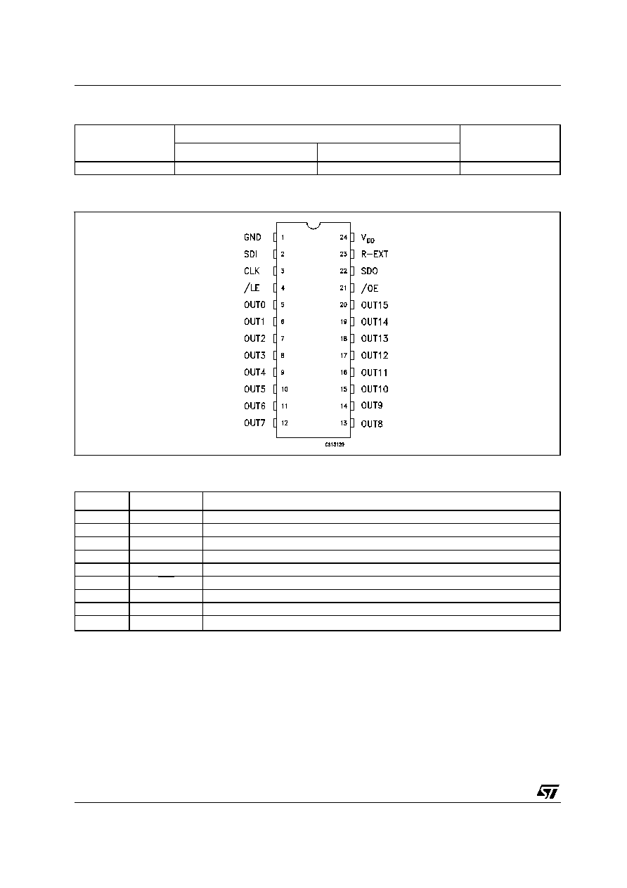
PIN CONNECTION
PIN DESCRIPTION
Output Voltage
Current accuracy
Output Current
Between bits
Between ICs
0.7V
± 6%
± 10%
2 to 90 mA
PIN N°
Symbol
Name and Function
1
GND
Ground Terminal
2
SDI
Serial data input terminal
3
CLK
Clock input terminal
4
/LE
Latch input terminal
5-20
OUT 0-15
Output terminal
21
/OE
Input terminal of output enable (active low)
22
SDO
Serial data out terminal
23
R-EXT
Input terminal of an external resistor for constant current programing
24
V
DD
Supply voltage terminal
STP16CL596
3/16
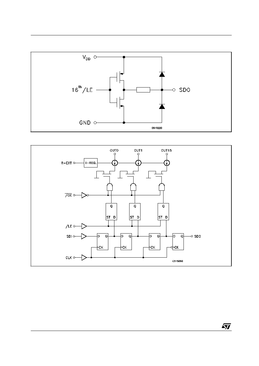
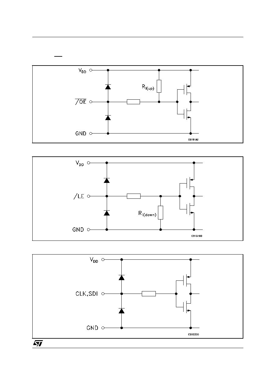
EQUIVALENT CIRCUIT OF INPUTS AND OUTPUTS
Figure 1 : /OE Terminal
Figure 2 : /LE Terminal
Figure 3 : CLK, SDI Terminal
STP16CL596
5/16
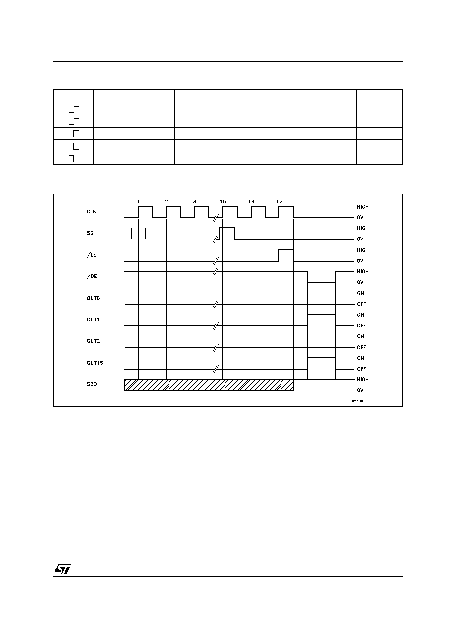
TRUTH TABLE
Note 1: OUT0 to OUT15 = ON when Dn = H; OUT0 to OUT15 = OFF when Dn = L.
TIMING DIAGRAM
Note: The latches circuit holds data when the LE terminal is Low.
When LE terminal is at High level, latch circuit doesn't hold the data it passes from the input to the output.
When OE terminal is at Low level, output terminals OUT0 to OUT15 respond to the data, either ON or OFF.
When OE terminal is at High level, it switches off all the data on the output terminal.
CLOCK
/LE
/OE
SERIAL-IN
OUT0 .................. OUT7 .................. OUT15
SDO
H
L
Dn
Dn ..... Dn - 7 ..... Dn -15
Dn - 15
L
L
Dn + 1
No Change
Dn - 14
H
L
Dn + 2
Dn - 2 ..... Dn - 5 ..... Dn -13
Dn - 13
X
L
Dn + 3
Dn - 2 ..... Dn - 5 ..... Dn -13
Dn - 13
X
L
Dn + 3
OFF
Dn - 13