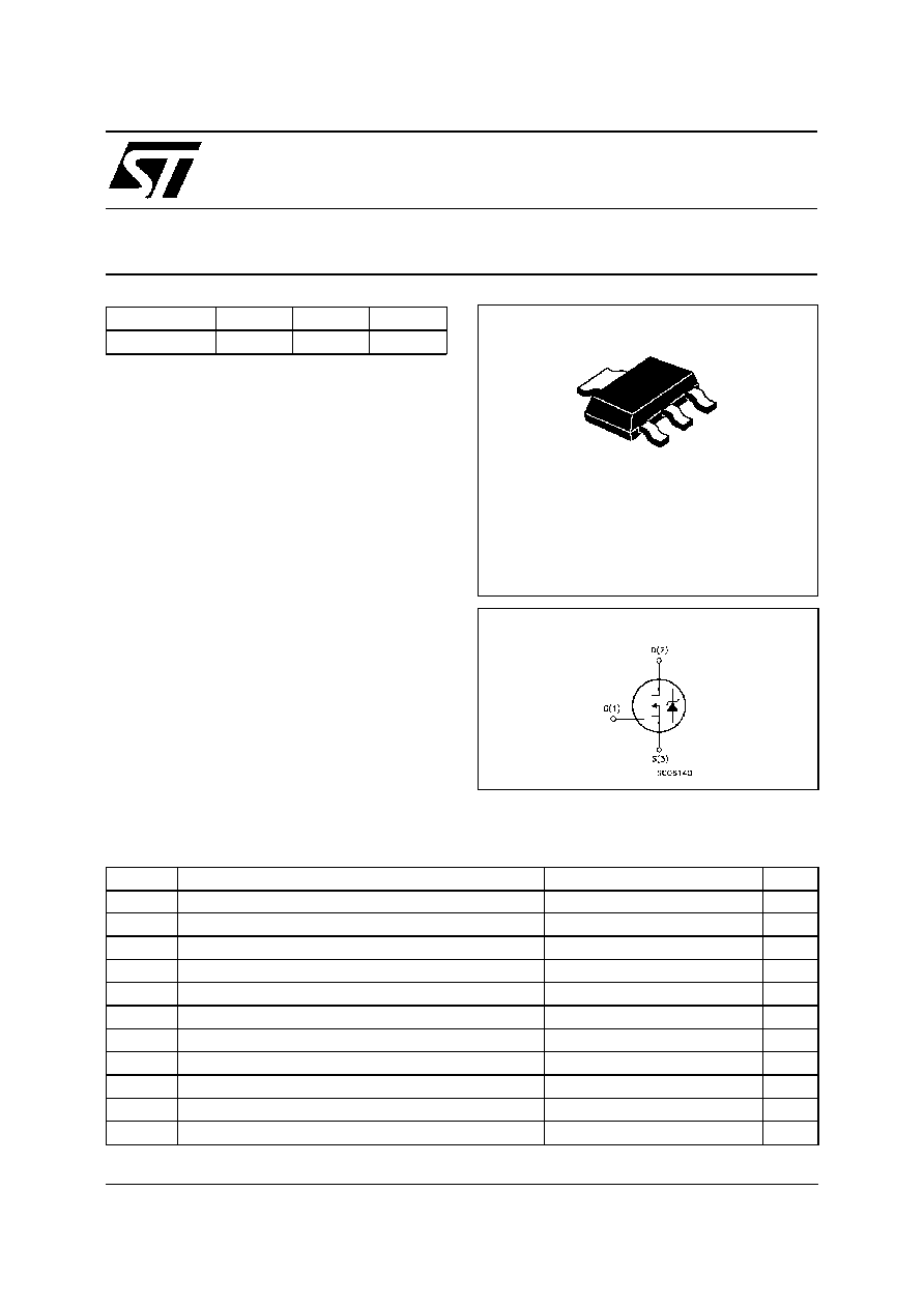
STN1NB80
N - CHANNEL 800V - 16
- 0.2A - SOT-223
PowerMESH
TM
MOSFET
s
TYPICAL R
DS(on)
= 16
s
EXTREMELY HIGH dv/dt CAPABILITY
s
100% AVALANCHE TESTED
s
VERY LOW INTRINSIC CAPACITANCES
s
GATE CHARGE MINIMIZED
DESCRIPTION
Using the latest high voltage MESH OVERLAY
TM
process, STMicroelectronics has designed an
advanced family
of
power MOSFETs
with
outstanding performances.
The
new
patent
pending strip layout coupled with the Company's
proprietary edge termination structure, gives the
lowest R
DS(on)
per area, exceptional avalanche
and dv/dt capabilities and unrivalled gate charge
and switching characteristics.
APPLICATIONS
s
SWITCH MODE POWER SUPPLIES (SMPS)
s
AC ADAPTORS AND BATTERY CHARGERS
FOR HANDHELD EQUIPMENT
INTERNAL SCHEMATIC DIAGRAM
November 1999
ABSOLUTE MAXIMUM RATINGS
Symbol
Parameter
Value
Un it
V
DS
Drain-source Voltage (V
GS
= 0)
800
V
V
DGR
Drain- gate Volt age (R
GS
= 20 k
)
800
V
V
GS
G ate-source Voltage
▒
30
V
I
D
Drain Current (continuous) at T
c
= 25
o
C
0.2
A
I
D
Drain Current (continuous) at T
c
= 100
o
C
0.12
A
I
DM
(
À
)
Drain Current (pulsed)
0.8
A
P
tot
T otal Dissipation at T
c
= 25
o
C
2.9
W
Derating Factor
0.02
W /
o
C
dv/dt (
1
)
Peak Diode Recovery volt age slope
4
V/ns
T
s tg
Storage Temperat ure
-65 to 150
o
C
T
j
Max. Operating Junction Temperature
150
o
C
(
À
) Pulse width limited by safe operating area
(
1
) I
SD
0.2 A, di/dt
200 A/
Á
s, V
DD
V
( BR)DSS
, Tj
T
JMAX
TYPE
V
DSS
R
DS(on)
I
D
ST N1NB80
800 V
< 20
0.2 A
SOT-223
«
1
2
2
3

THERMAL DATA
R
thj -case
Rthj -amb
R
thc-sink
T
l
Thermal Resistance Junction-case
Max
Thermal Resistance Junction-ambient
Max
Thermal Resistance Case-sink
Typ
Maximum Lead Temperature For Soldering Purpose
43
60
0.7
260
o
C/W
oC/ W
o
C/W
o
C
AVALANCHE CHARACTERISTICS
Symbo l
Parameter
Max Valu e
Unit
I
AR
Avalanche Current , Repet itive or Not-Repet itive
(pulse width limited by T
j
max)
0. 2
A
E
AS
Single Pulse Avalanche Energy
(starting T
j
= 25
o
C, I
D
= I
AR
, V
DD
= 50 V)
200
mJ
ELECTRICAL CHARACTERISTICS (T
case
= 25
o
C unless otherwise specified)
OFF
Symbo l
Parameter
Test Con ditions
Min.
T yp.
Max.
Unit
V
(BR)DSS
Drain-source
Breakdown Voltage
I
D
= 250
Á
A
V
GS
= 0
800
V
I
DSS
Zero G ate Voltage
Drain Current (V
GS
= 0)
V
DS
= Max Rating
V
DS
= Max Rating
T
c
= 125
o
C
1
50
Á
A
Á
A
I
G SS
Gat e-body Leakage
Current (V
DS
= 0)
V
GS
=
▒
30 V
▒
100
nA
ON (
)
Symbo l
Parameter
Test Con ditions
Min.
T yp.
Max.
Unit
V
G S(th)
Gat e Threshold
Voltage
V
DS
= V
GS
I
D
= 250
Á
A
3
4
5
V
R
DS(on)
Static Drain-source O n
Resist ance
V
GS
= 10V
I
D
=0.2 A
16
20
I
D(o n)
On Stat e Drain Current
V
DS
> I
D(o n)
x R
DS(on )ma x
V
GS
= 10 V
0. 2
A
DYNAMIC
Symbo l
Parameter
Test Con ditions
Min.
T yp.
Max.
Unit
g
f s
(
)
Forward
Transconduct ance
V
DS
> I
D(o n)
x R
DS(on )ma x
I
D
= 0.2 A
0. 1
0.4
S
C
iss
C
os s
C
rss
Input Capacitance
Out put Capacitance
Reverse T ransfer
Capacitance
V
DS
= 25 V
f = 1 MHz
V
GS
= 0
140
22
2.5
pF
pF
pF
STN1NB80
2/8
ELECTRICAL CHARACTERISTICS (continued)
SWITCHING ON
Symbo l
Parameter
Test Con ditions
Min.
T yp.
Max.
Unit
t
d(on)
t
r
Turn-on delay Time
Rise Time
V
DD
= 400 V
I
D
= 0.5 A
R
G
= 4.7
V
G S
= 10 V
(see test circuit, figure 3)
8
10
ns
ns
Q
g
Q
gs
Q
gd
Tot al Gate Charge
Gat e-Source Charge
Gat e-Drain Charge
V
DD
= 640 V
I
D
=1. 1 A V
G S
= 10 V
10
5
3.6
14
nC
nC
nC
SWITCHING OFF
Symbo l
Parameter
Test Con ditions
Min.
T yp.
Max.
Unit
t
r (Voff)
t
f
t
c
Off -volt age Rise Time
Fall Time
Cross-over Time
V
DD
= 640 V
I
D
= 1.1 A
R
G
= 4.7
V
GS
= 10 V
(see test circuit, figure 5)
40
16
50
ns
ns
ns
SOURCE DRAIN DIODE
Symbo l
Parameter
Test Con ditions
Min.
T yp.
Max.
Unit
I
SD
I
SDM
(
À
)
Source-drain Current
Source-drain Current
(pulsed)
0. 2
0. 8
A
A
V
SD
(
)
Forward On Volt age
I
SD
=0.2 A
V
GS
= 0
1. 6
V
t
rr
Q
rr
I
RRM
Reverse Recovery
Time
Reverse Recovery
Charge
Reverse Recovery
Current
I
SD
= 1.1 A
di/dt = 100 A/
Á
s
V
DD
= 100 V
T
j
= 150
o
C
(see test circuit, figure 5)
460
1150
5
ns
Á
C
A
(
) Pulsed: Pulse duration = 300
Á
s, duty cycle 1.5 %
(
À
) Pulse width limited by safe operating area
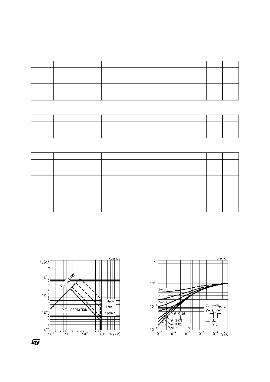
Safe Operating Area
Thermal Impedance
STN1NB80
3/8
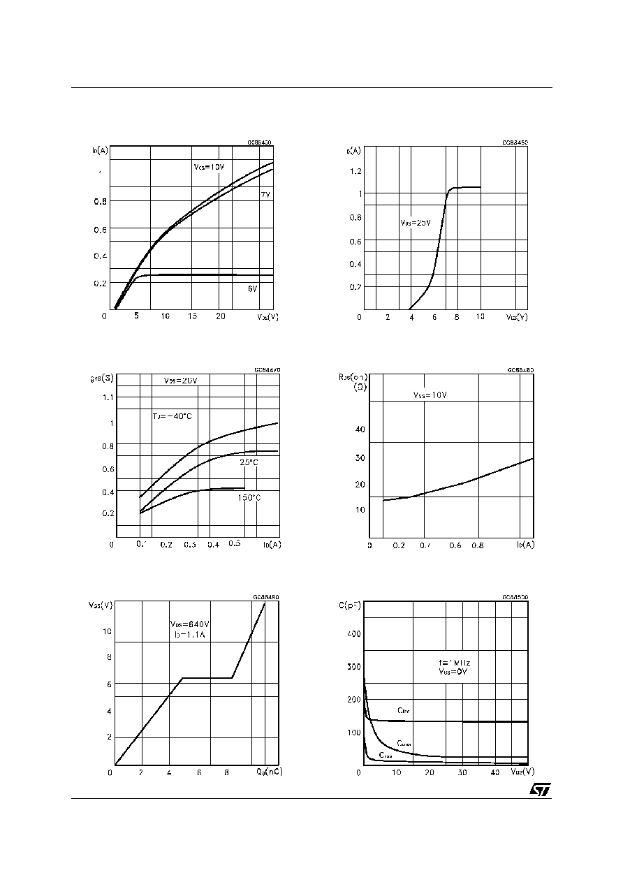
Output Characteristics
Transconductance
Gate Charge vs Gate-source Voltage
Transfer Characteristics
Static Drain-source On Resistance
Capacitance Variations
STN1NB80
4/8
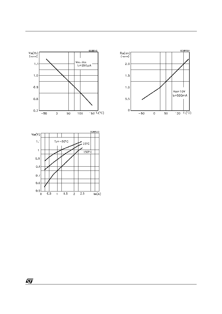
Normalized Gate Threshold Voltage vs
Temperature
Source-drain Diode Forward Characteristics
Normalized On Resistance vs Temperature
STN1NB80
5/8