RF POWER MODULE
WIRELESS LOCAL LOOP APPLICATIONS
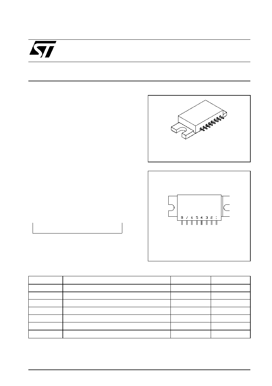
CASE STYLE H170
.
LINEAR POWER AMPL IFIER
.
325-351 MHz
.
20 VOLTS
.
INPUT/OUTPUT 50 OHMS
.
P
OU T
=
1.0 W
AV G
(2.0 W PEP)
.
GAIN
=
21 dB
DESCRIPTION
The STM351-2 module is designed to be used
as a linear RF Power Amplifier for WLL or other
fixed radio a ccess subscriber applications.
This particular model is one of several in de-
sign cover ing the 300-5 00 MHz freque ncy
range in individual
bandwidths of 25 MHz
each.
Band splits and corresponding part numbers
for all bands are as follows:
PIN CONNECTION
ORDER CODE
BRANDING
STM351-2
STM351-2
ABSOLUTE MAXIMUM RATINGS (T
case
=
25
°
C)
Symbol
Parameter
Valu e
Uni t
V
CC
DC Supply Voltage
+21
Vdc
I
CC (q)
Quiescent Current (pin 7)
200
mAdc
I
CC
Operating Current (pin 7)
500
mAdc
P
IN
RF Input Po wer
30
mW
P
OU T
RF Output Power
2.0
W
AVG
T
ST G
Storage Temperature
-30 to +100
°
C
T
C
Operating Case Temperature
-
20 to +60
°
C
STM351-2
1. RF Input
5. I
BB
2. N/C
6. GND
3. GND
7. V
CC
(+20VDC)
4. N/C
8. RF output
PRELIMI NARY DATA
STM326-2
300-326 MHz
STM351-2
325-351 MHz
PROTOTYPES
STM376-2
350-376 MHz
AVAILABLE
STM401-2
375-401 MHz
STM426-2
400-426 MHz
STM451-2
425-451 MHz
STM476-2
450-476 MHz
STM500-2
475-500 MHz
®
June 15, 1998
1/3

ELECTRICAL SPECIFICATIONS (T
case
=
30
°
C, V
CC
=
20.0Vdc, V
BB
=
8.8 Vdc)
Symb ol
Parameter
Test Con dition s
Value
Uni t
Min.
Typ.
Max.
BW
Frequency Range
325
--
351
MHz
G
P
Power Gain
P
OUT
=
1.0 W*
21
23
25
dB
Efficiency
P
OUT
=
1.0 W*
11
12.5
--
%
Input VSWR
P
OUT
=
1.0 W*
Z
S
, Z
L
=
50
--
--
1.5:1
VSWR
I
CC( q)
Quiescent
Current
P
IN
=
0 W
110
120
130
mA
I
CC
Collector Supply
Current
P
OUT
=
1.0 W*
--
375
425
mA
I
BB
Bias Current
P
OUT
=
1.0 W*
--
65
--
mA
H
Harmonics
P
OUT
=
1.0 W*
F = 325 MHz
--
-34
-30
dBc
IMD
Inte rmodulation
Distortion
P
OUT
=
1.0 W*
-46
-40
dBc
--
Load Mismatch
Load VSWR
=
:1
(All phase angles)
P
OUT
=
1.0 W*
No Degradation in Output
Power after Load Restoration
--
Stability
Load VSWR
=
5:1
(All phase angles)
P
OUT
=
1.0 W*
All Spurious outputs more
than 50dB below carrier
* 2 T one Test, 50 KHz spacing: P
OUT
= 1.0 W
AVG
(2. 0 W
PEP
)
MODULE DC AND TEST FIXTURE CONFIGURATION
1 2 3 4 5 6 7 8
N/C
N/C
RF
IN
RF
OUT
50
Line
50
Line
120
1 W
10 uF
3.3 uF
1000 pF
0.1 uF
+8.8VDC
+20 VDC
* Bead
300 pF
300 pF
1000 pF
®
STM351-2
2/3
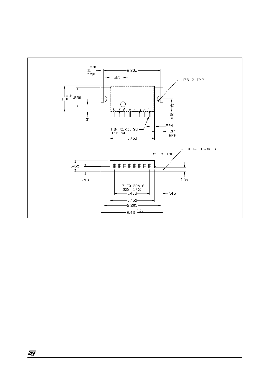
PACKAGE MECHANICAL DATA
Informati on furni shed i s believed to be accurate and reliable. H owever , STMicroelectroni cs assumes no responsibi lity for the conse -
quences of use of such i nformation nor for any infri ngement of patents or other rights of thir d parties which may result from its use. No
license is granted by implication or otherwise under any patent or patent r ig hts of STMicroelectronics. Specifications mentioned in this
publication are subject to change without notice. T his publication supersedes and replac es all information previously suppl ied.
STMicr oelectronics products are not authori zed for use as critical components i n li fe suppo rt devi ces or systems without express written
approval of STMicroelectronics.
The ST l ogo is a registered trademark of STMicroelectronics
©
1998 STM icroel ectronics - Al l R ights Reserved
ST Microelectronics GRO UP OF COMPANIES
Australia - Brazil - Canada - China - France - Germany - Italy - Japan - Korea
Malaysi a - Malta - Mexico - Morocco - The Netherlands - Si ngapore - S pain - Sweden - Swi tzerl and
Taiwan - Thailand - United Ki ngdom - U.S.A.
Ref.: UDCS No. 1021374 rev. A
®
STM351-2
3/3