STLC7550
LOW POWER LOW VOLTAGE ANALOG FRONT END
November 1998
TQFP44 (10 x 10 x 1.40 mm)
(Full Plastic Quad Flat Pack)
ORDER CODE : STLC7550TQFP
.
GENERAL PURPOSE SIGNAL PROCESSING
ANALOG FRONT END (AFE)
.
TARGETED FOR V.34bis MODEM AND
56Kbps MODEM APPLICATIONS
.
16-BIT OVERSAMPLING
A/D AND D/A
CONVERTERS
.
83dB SIGNAL TO NOISE RATIO FOR SAM-
PLING FREQUENCY UP TO 9.6kHz @ 3V
.
87dB DYNAMIC RANGE @ 3V
.
FILTER BANDWIDTHS :
0.425 x THE SAMPLING FREQUENCY
.
ON-CHIP REFERENCE VOLTAGE
.
SINGLE POWER SUPPLY RANGE :
2.7 TO 5.5V
.
LOW POWER CONSUMPTION LESS THAN
30mW OPERATING POWER 3V
.
STAND-BY MODE POWER CONSUMPTION
LESS THAN 3
�
W at 3V
.
PROGRAMMING SAMPLING FREQUENCY
.
MAX. SAMPLING FREQUENCY : 45kHz
.
SYNCHRONOUS SERIAL INTERFACE FOR
PROCESSOR DATAS EXCHANGE. MASTER
OR SLAVE OPERATIONS
.
0.50
�
m CMOS PROCESS
.
TQFP44 PACKAGE
.
STLC7546 MODE OF OPERATION COMPATIBLE
DESCRIPTION
The STLC7550 is a single chip Analog Front-end
(AFE) designed to implement modems up to
56Kbps.
It has been especially designed for host processing
application in which the modulation software
(V.34bis, 56Kbps) is performed by the main applica-
tion processor : Pentium, Risc or DSP processors.
The main target of this device is stand alone appli-
ances as Hand Held PC (HPC), Personnal Digital
Assistants (PDA), Webphones, Network Comput-
ers, Set Top Boxes for Digital Television (Satellite
and Cable).
To comply with such applications STLC7550 is
powered nominally at 3V only.
Maximum Power Dissipation 30mW is well suited
for Battery operations.
In case of battery low, STLC7550 will continue to
work even at a 2.7V level.
STLC7550 also provides clock generator for all
sampling frequencies requested for V.34bis and
56Kbps applications.
This new AFE can also be used for PC mother
boards or add-on cards or stand alone MODEMs.
It can be used in a master mode or slave mode.
The slave mode eases multi AFE architecture de-
sign in saving external logical glue.
TQFP48 (7 x 7 x 1.40mm)
(Full Plastic Quad Flat Pack)
ORDER CODE : STLC7550TQF7
1/17

44
43
42
41
40
39
38
37
36
35
34
12
13
14
15
16
17
18
19
20
21
22
1
2
3
4
5
6
7
8
9
10
11
23 24 25 26 27 28 29 30 31 32 33
DOUT
DIN
TSTD1
TS
RESET
OUT-
OUT+
AGND2
V
CM
AV
DD
IN-
IN+
AUXIN+
AUXIN-
AGND1
V
REFN
M/S
V
REFP
PWRDWN
HC0
HC1
XTALIN/MCLK
XTALOUT
MCM
DGND
DV
DD
FS
SCLK
75
50
-
0
1.
E
P
S
PIN CONNECTIONS (TQFP44)
1
2
3
4
5
6
7
8
9
10
11
25 26 27 28 29 30 31 32 33
12
34 35 36
13
14
15
16
17
18
19
20
21
22
23
24
44
43
42
41
40
39
38
37
45
46
47
48
AGND2
V
CM
AV
DD
IN-
IN+
AUXIN+
AUXIN-
XTALIN/MCLK
XTALOUT
MCM
DGND
DV
DD
FS
SCLK
DOUT
DIN
TSTD1
TS
RESET
OUT-
OUT+
AGND1
V
REFN
M/S
V
REFP
PWRDWN
HC0
HC1
7
5
5
0
-0
1
.
EPS
PIN CONNECTIONS (TQFP48)
STLC7550
2/17
PIN LIST
Pin Number
Name
Type
Description
TQFP44
TQFP48
1 - 2, 10 to 13,
21 to 24, 32 to
35, 43 - 44
1 - 2, 10 to 14,
22 to 26, 34 to
38, 46 to 48
NC
-
Not connected
3
3
SCLK
O
Shift Clock Output
4
4
FS
I/O
Frame Synchronization Input (slave)/Output (master)
5
5
DV
DD
I
Positive Digital Power Supply (2.7V TO 5.5V)
6
6
DGND
I
Digital Ground
7
7
MCM
I
Master Clock Mode
8
8
XTALOUT
O
Crystal Output
9
9
XTALIN/MCLK
I
Crystal Input (MCM = 1) / External Clock (MCM = 0)
14
15
HC1
I
Hardware Control Input
15
16
HC0
I
Hardware Control Input
16
17
PWRDWN
I
Power down Input
17
18
M/S
I
Master/Slave Mode Control Pin Input
18
19
V
REFP
O
16-bit D/A and A/D Positive Reference Voltage
19
20
V
REFN
O
16-bit D/A and A/D Negative Reference Voltage
20
21
AGND1
I
Analog Ground
25
27
AUXIN+
I
Non-inverting Input to Auxiliary Analog Input
26
28
AUXIN-
I
Inverting Input to Auxiliary Analog Input
27
29
IN+
I
Non-inverting Input to Analog Input Amplifier
28
30
IN-
I
Inverting Input to Analog Input Amplifier
29
31
AV
DD
I
Positive Analog Power Supply (2.7V to 5.5V)
30
32
V
CM
O
Common Mode Voltage Output (AV
DD
/2)
31
33
AGND2
I
Analog Ground
36
39
OUT+
O
Non-inverting Smoothing Filter Output
37
40
OUT-
O
Inverting Smoothing Filter Output
38
41
RESET
I
Reset Function to initialize the internal counters
39
42
TS
I
Timeslot Control Input
40
43
TSTD1
I/O
Digital Input/Output reserved for test
41
44
DIN
I
Serial Data Input
42
45
DOUT
O
Serial Data Output
75
50
-
0
1.
T
B
L
PIN DESCRIPTION
1 - POWER SUPPLY (5 pins)
1.1 - Analog V
DD
Supply (AV
DD
)
This pin is the positive analog power supply
voltage for the DAC and the ADC section.
It is not internally connected to digital V
DD
supply
(DV
DD
).
In any case the voltage on this pin must be higher
or equal to the voltage of the Digital power supply
(DV
DD
).
1.2 - Digital V
DD
Supply (DV
DD
)
This pin is the positive digital power supply for DAC
and ADC digital internal circuitry.
1.3 - Analog Ground (AGND1, AGND2)
These pins are the ground return of the analog DAC
(ADC) section.
1.4 - Digital Ground (DGND)
This pin is the ground for DAC and ADC internal
digital circuitry.
Notes : 1. To obtain published performance, the analog V
DD
and Digital V
DD
should be decoupled with respect to Analog Ground and Digital
Ground, respectively. The decoupling is intended to isolate digital noise from the analog section ; decoupling capacitors should
be as close as possible to the respective analog and digital supply pins.
2. All the ground pins must be tied together. In the following section, the ground and supply pins are referred to as GND and V
DD
,
respectively.
STLC7550
3/17

2 - HOST INTERFACE (10 pins)
2.1 - Data In (DIN)
In Data Mode, the data word is the input of the DAC
channel. In software, the data word is followed by
the control register word.
2.2 - Data Out (DOUT)
In Data Mode, the data word is the ADC conversion
result. In software, the data word is followed by the
register read.
2.3 - Frame Synchronization (FS)
In master mode, the frame synchronization signal
is used to indicate that the device is ready to send
and receive data. The data transfer begins on the
falling edge of the frame-sync signal. The frame-
sync is generated internally and goes low on the
rising edge of SCLK in master mode. In slave mode
the frame is generated externally.
2.4 - Serial Bit Clock (SCLK)
SCLK clocks the digital data into DIN and out of
DOUT during the frame synchronization interval.
The Serial bit clock is generated internally.
2.5 - Reset Function (RESET)
The reset function is to initialize the internal count-
ers and control register. A minimum low pulse of
100ns is required to reset the chip. This reset
function initiates the serial data communications.
The reset function will initialize all the registers to
their default value and will put the device in a
pre-programmed state. After a low-going pulse on
RESET, the device registers will be initialized to
provide an over-sampling ratio equal to 160, the
serial interface will be in data mode, the DAC
attenuation will be set to infinite, the ADC gain will
be set to 0dB, the Differential input mode on the
ADC converter will be selected, and the multiplexor
will be set on the main inputs IN+ and IN-. After a
reset condition, the first frame synchronization cor-
responds to the primary channel.
2.6 - Power Down (PWRDWN)
The Power-Down input powers down the entire
chip (< 50
�
W). When PWRDWN Pin is taken low,
the device powers down such that the existing
internally programmed state is maintained. When
PWRDWN is driven high, full operation resumes
after 1ms. If the PWRDWN input is not used, it
should be tied to V
DD
.
2.7 - Hardware Control (HC0, HC1)
These two pins are used for Hardware/Software
Control of the device. The data on HC0 and HC1
will be latched on to the device on the rising edge
of the Frame Synchronization Pulse. If these two
pins are low, Software Control Mode is selected.
When in Software Control Mode, the LSB of the
16-bit word will select the Data Mode (LSB = 0) or
the Control Mode (LSB = 1). Other combinations of
HC0/HC1 are for Hardware Control. These inputs
should be tied low if not used.
2.8 - Master/Slave Control (M/S)
When M/S is high, the device is in master mode
and Fs is generated internally. When M/S is low,
the device is in slave mode and Fs must be
generated externally.
2.9 - Master Clock Mode (MCM)
When MCM is high, XTALIN is provided externally
and must be equal to 36.864MHz. When MCM is low,
XTALIN is provided externally and must be equal to
oversampling frequency : Fs x Over (see Clock Block
Diagram and �4 Modes of Operation).
2.10 - Timeslot Control (TS)
When TS = 0 the data are assigned to the first
16 bits after falling edge of FS (7546 mode) other-
wise the data are bits 17 to 32.
The case M/S = 1 with TS = 1 is reserved for life-test
(transmit gain fixed to 0dB).
3 - CLOCK SIGNALS (2 pins)
Depending on MCM value, these pins have differ-
ent function.
3.1 - MCM = 1 (XTALIN, XTALOUT)
These pins must be tied to external crystal. For the
value of crystal see Functional Description Chapter
Part 3.
3.2 - MCM = 0 (MCLK, XTALOUT)
MCLK Pin must be connected to an external clock.
XTALOUT is not used.
PIN DESCRIPTION (continued)
STLC7550
4/17
4 - ANALOG INTERFACE (9 pins)
4.1 - DAC and ADC Positive Reference
Voltage Output (V
REFP
)
This pin provides the Positive Reference Voltage
used by the 16-bit converters. The reference volt-
age, V
REF
, is the voltage difference between the
V
REFP
and V
REFN
outputs, and its nominal value is
1.25V. V
REFP
should be externally decoupled with
respect to V
CM
.
4.2 - DAC and ADC Negative Reference
Voltage Output (V
REFN
)
This pin provides the Negative Reference Voltage
used by the 16-bit converters, and should be exter-
nally decoupled with respect to V
CM
.
4.3 - Common Mode Voltage Output (V
CM
)
This output pin is the common mode voltage
(AV
DD
- AGND)/2. This output must be decoupled
with respect to GND.
4.4 - Non-inverting Smoothing Filter Output(OUT+)
This pin is the non-inverting output of the fully
differential analog smoothing filter.
4.5 - Inverting Smoothing Filter Output (OUT-)
This pin is the inverting output of the fully differential
analog smoothing filter. Outputs OUT+ and OUT-
provide analog signals with maximum peak-to-
peak amplitude 2 x V
REF
, and must be followed by
an external two pole smoothing filter. The external
filter follows the internal single pole switch capaci-
tor filter. The cutoff frequency of the external filter
must be greater than two times the sampling fre-
quency (FS), so that the combined frequency re-
sponse of both the internal and external filters is flat
in the passband . The attenuator of the last output
stage can be programmed to 0dB, 6dB or infinite.
4.6 - Non-inverting Analog Input (IN+)
This pin is the differential non-inverting ADC input.
4.7 - Inverting Analog Input (IN-)
This pin is the differential inverting ADC input.
These analog inputs (IN+, IN-) are presented to the
Sigma-Delta modulator. The analog input peak-to-
peak differential signal range must be less than
2 x V
REF
, and must be preceded by an external
single pole anti-aliasing filter. The cut-off frequency
of the filter must be lower than one half the over-
sampling frequency. These filters should be set as
close as possible to the IN+ and IN- pins. The gain
of the first stage is programmable (see Table 3).
4.8 - Non-inverting Auxiliary Analog
Input (AUX IN+)
This pin is the differential non-inverting auxiliary ADC
input. The characteristics are same as the IN+ input.
4.9 - Inverting Auxiliary Analog Input (AUX IN-)
This pin is the differential inverting auxiliary ADC
input. The characteristics are same as the IN- input.
The input pair (IN+/IN- or AUX IN+/AUX IN-) are
software selectable.
PIN DESCRIPTION (continued)
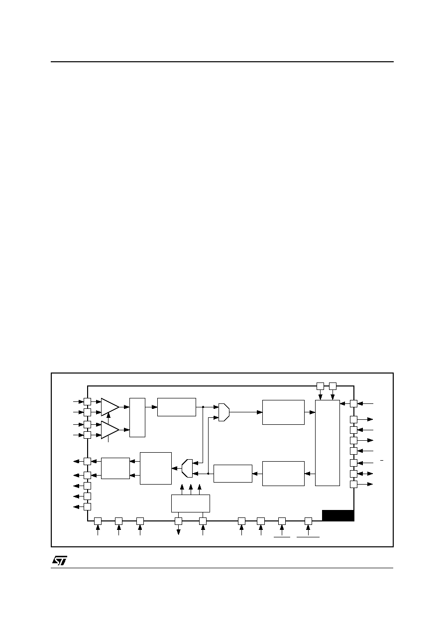
ANALOG
MODULATOR
2nd ORDER
MODULATOR
LOW-PASS
(0.425 x sampling
frequency)
HC0
OUT+
OUT-
V
CM
V
REFN
V
REFP
IN+
IN-
(0 + 6dB in
diff. input)
DAC 1 BIT
First order
differential
switched
capacitor
filter
LOW-PASS
(0.425 x sampling
frequency)
SERIAL PORTS
AND CONTROL REGISTER
ATTEN.
0dB/+6dB/
INFINITE
M/S
FS
SCLK
DOUT
DIN
CLOCK
GENERATOR
XTALIN
XTALOUT
AGND2
AGND1
AV
DD
DV
DD
DGND
STLC7550
RESET
PWRDWN
38
16
6
5
9
8
31
20
29
37
36
30
19
18
28
27
15
TS
7
MCM
39
HC1
14
17
4
3
42
41
TSTD1
40
AUXIN+
AUXIN-
26
25
MUX
7
5
5
0
-0
2
.
EPS
BLOCK DIAGRAM (TQFP44)
STLC7550
5/17