STLC5444
QUAD FEEDER POWER SUPPLY
SUPPLIES POWER FOR UP TO FOUR DIGI-
TAL TELEPHONE LINES
CONFORMS TO THE CCITT RECOMMEN-
DATIONS FOR POWER FEED AT THE S OR
T REFERENCE POINTS
SUPPORTS POINT-TO-POINT AND POINT
TO MULTIPOINT CONFIGURATIONS
EACH OF THE FOUR LINES IS INDIVIDU-
ALLY CONTROLLED
HIGH-VOLTAGE BCD TECHNOLOGY SUP-
PORTING UP TO -130V
AUTOMATIC THERMAL SHUTDOWN
STATUS CONDITION DETECTION (BY MI-
CROPROCESSOR) FOR EACH LINE:
Low output voltage
Openloop
Current overload
Thermal overload
Normal line condition
PROGRAMMABLE CURRENT LIMITING
OUTPUT CURRENT UP TO 120mA
DESCRIPTION
The ISDN Quad Feeder Power Supply (IQFPS)
provides a power source for up to four line inter-
faces. The power source to the device is a local
battery or a centralized regulated power supply.
It can operate in point-to-point and point-to-mul-
tipoint configurations as far as S interface is con-
cerned.
By the device microprocessor interface, each
powered line is individually controlled and moni-
tored.
Therefore, overloads and faults are easy to detect
and localize even in a large system.
The status conditions detected by the device on
each line that may be read by the microprocessor
are :
low output voltage
openloop
current overload
thermal overload
normal line conditions
A hardware current limiting programmable feature
is available.
December 1997
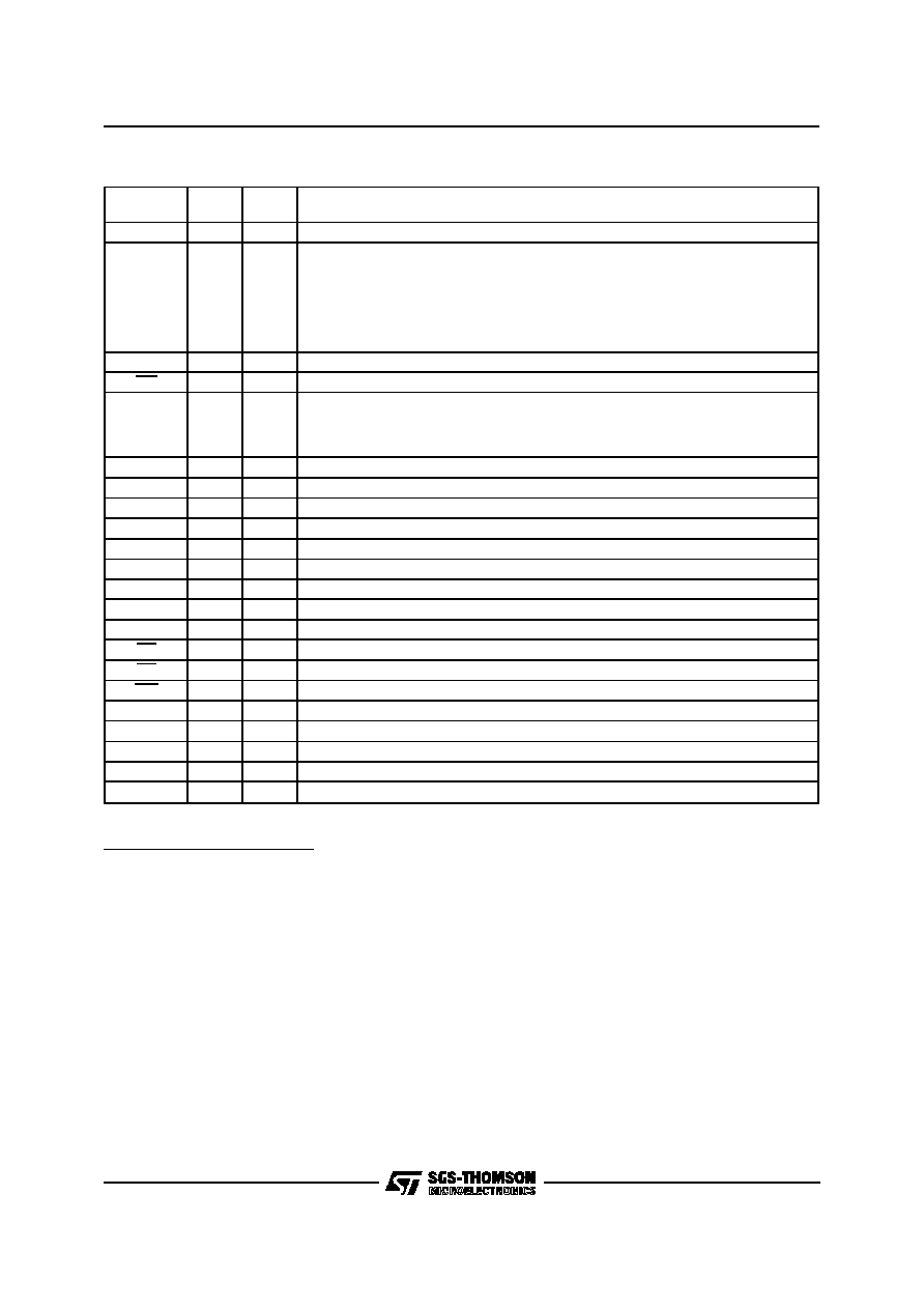
DIP24
PLCC44
ORDERING NUMBERS: STLC5444B1 (DIP24)
STLC5444FN (PLCC44)
ILIM
N.C.
VBB
N.C.
S0
VBB
S1
1
3
2
4
5
6
7
8
9
S2
S3
RSRVD
RESET
RD
CS
WR
19
18
17
16
15
13
14
D94TL102
10
11
12
24
23
22
21
20
D1
D0
INT
BGND
VCC
ALE
DGND
A0
D3
D2
DIP24 PIN CONNECTION (Top view)
1/17

1
2
3
5
6
4
7
8
9
10
12
11
13
14
15
16
17
39
38
37
36
34
35
33
32
31
30
29
40
41
42
44 43
23
22
21
19
18
20
28
27
26
24 25
D1
N.C.
D0
INT
VBB
N.C.
VBB
A0
D3
N.C.
D2
VBB
N.C.
BGND
N.C.
ILIM
VCC
N.C.
N.C.
VBB
N.C.
VBB
VBB
N.C.
N.C.
DGND
N.C.
ALE
WR
CS
RD
RESET
VBB
N.C.
VBB
S1
S0
N.C.
N.C.
N.C.
S3
N.C.
S2
N.C.
D94TL103
PLCC44 PIN CONNECTION (Top view)
MUX
INDIRECT
ADDRESS
REGISTER
µ
P
INTERFACE
ADDRESS
BUS 0/2
BIT 3
INT EN
OUTPUT
BUS D3/D0
IAR EN
LINE
ENABLE
REGISTER
INPUT BUS D3/D0
VOLTAGE
REFERENCE
S
DRIVERS
STATUS
DETECTOR
STATUS GROUP BUS
LINE ENABLE REGISTER BUS
LER EN
S DRIVERS
DISABLE
O/3
D94TL104B
THERMAL
OVERLOAD
LINE
STATUS
BUS
ALE
A0
CS
D3/D0
RD
WR
INT
RESET
ILIM
VBB(8)
VCC
DGND
BGND
VBB(12)
S3
S2
S1
S0
BLOCK DIAGRAM
STLC5444
2/17
PIN DESCRIPTION
Name
N
o
PLCC
N
o
DIP
Function
D1
1
1
Bit 1 of the tri state I/O data bus
NC
2,4,8,10,
13,14,
16,18,
20,23,
25,26,
28,34,
37,38,44
7,9
No connection
D0
3
2
Bit 0 of the tri state I/O data bus
INT
5
3
Active low interrupt output for the
µ
P (open drain)
VBB
6,7
15,17
22,29,
39,40
8,12
Battery supply line (negative battery`s terminal)
BGND
9
4
Battery ground line
VCC
11
5
+5V supply line
ILIM
12
6
Current limit programming
S0
19
10
Output of the power switch controller 0
S1
21
11
Output of the power switch controller 1
S2
24
13
Output of the power switch controller 2
RSRVD
14
Reserved pin: it must be left floating
S3
27
15
Output of the power switch controller 3
RESET
30
16
Active high reset input
RD
31
17
Active low read input
CS
32
18
Active low chip select input
WR
33
19
Active low write input
ALE
35
20
Active high address latch enable
DGND
36
21
Digital ground
A0
41
22
Address bit for R/W operations on the data bus
D3
42
23
Bit 3 of the I/O tri state data bus
D2
43
24
Bit 2 of the I/O tri state data bus
FUNCTIONAL DESCRIPTION
ADDRESS LINE (Input)
A0 selects source and destination locations for
read and write operations on the data bus. A0
must be valid on the falling edge of ALE or during
RD and WR if ALE is tied High.
ALE - Address Latch Enable (Input; Active
High)
ALE is an input control pulse used to strobe the
address on the A0 line into the address latch.
This signal is active High to admit the input ad-
dress. The address is latched on the High-Low
transition of ALE. While ALE is High, the address
latch is transparent. For an unmultiplexed micro-
processor bus, ALE must be tied High.
BGND - Ground Battery
CS - Chip Select (Input; Active Low)
CS must be Low to enable the read or write op-
erations of the device. Data transfer occurs over
the D3-D0 lines.
D3-D0 - DATA BUS (Input/Output; Three-State)
The four bidirectional data bus lines are to ex-
change information with a microprocessor. D0 is
the least significant bit and D3 is the most signifi-
cant bit. A High on the data bus corresponds to a
logical 1. These lines act as input when WR and
CS are active and as output when RD and CS are
active. When CS is inactive, the D3-D0 pins are
placed in a high-impedance state.
STLC5444
3/17

FUNCTIONAL DESCRIPTION (continued)
DGND - Ground Digital
ILIM - Current Limit Programming (Input)
ILIM programs the current limit of the Output driv-
ers using an external resistor connected between
ILIM and VBB. The ILIM pin is 1.25V more posi-
tive than VBB. The current limit is 5mA plus 1000
times the current in the external resistor. The pro-
grammed current limit applies to each driver.
INT - Interrupt (Output; Open-Collector, Active
Low)
INT augments the Microprocessor Interface by
generating an interrupt when a Current Overload
Detector (COD) occurs. INT is active whenever
any bits in the COD register are active. INT is not
latched; when the COD register is zero, INT goes
inactive (High). INT will also go inactive if the
IQFPS automatically disables the S-output driver
that caused the interrupt (due to Thermal Over-
load), or if the microprocessor disables that line
via the Line Enable Register (LER). COD inter-
rupts can be masked via the Indirect Address
Register (IAR); RESET always disables the INT
pin.
RD - Read (Input; Active Low)
The active Low read signal is conditioned by CS
and transfers internal information to the data bus.
If A0 is a logical 0, logic levels of the Indirect Ad-
dress Register (IAR) and Thermal Shutdown
Status bit will be transferred to D3-D0. If A0 is a
logical 1, the data addressed by the IAR will be
transferred to D3-D0.
RESET - Reset (Input; Active High)
RESET initialize the registers in the device, leav-
ing the drivers switched off.
S3-S0 - Drivers (Output)
S3-S0 each supply power to one line. The outputs
can sink up to 120 mA each. The voltage at the
line is connected to VBB through a DMOS switch.
VBB - Battery Voltage (input)
VBB is the internal negative supply voltage. VBB
must always be connected to the most negative
supply voltage. The MPI Registers will not func-
tion properly when the battery power is discon-
nected, that is, when VBB is floating or grounded.
The IQFPS should also be reset if a drastic tran-
sient is applied to VBB.
VCC - +5V Power Supply (Input)
WR - Write (Input; Active Low)
The active Low write signal is conditioned by CS
and transfers information from the data bus to an
internal register selected by A0. If A0 is a logical
1, D3-D0 is written into the Line Enable Register
(LER). If A0 is a logical 0, D3-D0 is written into
the IAR. LER and IAR are the only two writable
registers in the device.
STLC5444
4/17
DC CHARACTERISTICS (V
BB
= -54V; V
CC
= 5V; unless otherwise specified)
Symbol
Parameter
Test Conditions
Min.
Typ.
Max.
Unit
V
IH
Input Voltage High Level
2
V
V
IL
Input Voltage Low Level
0.8
V
I
OH
High Level Output Current
V
OH
= 2.4V
400
µ
A
I
OL
Low Level Output Current
V
OL
= 0.4V
2
mA
I
IH
High Level Input Current
V
IH
= 2V
10
µ
A
I
IL
Low Level Input Current
V
IL
= 0.8V
60
µ
A
I
OZH
Output Hi-Z Current High
2.4V < V
OZ
< V
CC
10
µ
A
I
OZL
Output Hi-Z Current Low
0V < V
OZ
< 0.4V
10
µ
A
I
CC
V
CC
supply Current
1.4
5
mA
C
L
Logic I/O Capacitance
10
pF
V
SAT
Saturation Voltage
I
S
= 80mA
2
V
R
on
Output DMOS Saturation Resistivity
I
S
= 80mA
25
I
BB
V
BB
Supply Current
V
BB
= -54V, R
LI M
= 26.6K
,
Output Disabled
3.2
6
mA
I
SLIM
Delta Limit Current vs.
Theoretical Programmed Value
I
SLIM
R
LIM
= 26.6K
, V
BB
= -96V
R
LIM
= 10.9K
, V
BB
= -54V
±
10%
V
LVD
Low Voltage Detector Threshold
(relative to V
BB
)
S3 - S0 output active
2.7
3
3.3
V
I
SOL
Current Overload Detector
Threshold (as % of I
SLIM
)
75
90
%
I
SOC
Open Loop Detector Threshold
1.5
3
4
mA
I
SZ
Si Leakage Current to ground @
Si disabled
V
BB
= -110V
100
µ
A
H
LVD
Low Voltage Detector Hysteresis
18
200
mV
H
OLD
Open Loop Detector Hysteresis
0.6
1.6
mA
H
COD
Current Overload Detector
Hysteresis
2.4
4.0
mA
H1
130
°
C Thermal Detector
Hysteresis
10
°
C
H2
160
°
C Thermal Detector
Hysteresis
10
°
C
T
H1
Thermal Overload Recovery
Time H1
80
µ
s
STLC5444
5/17