PROGRAMMABLE MONOLITHIC 4 CHAN-
NEL CODEC/FILTER
SINGLE +3.3V SUPPLY
PIN STRAP / MCU CONTROL MODE
A/
Á
LAW PROGRAMMABLE
LINEAR CODING (16 BITS) OPTION
PCM HIGHWAY FORMAT AUTOMATICALLY
DETECTED: 1.536 or 1.544MHz; 2.048, 4.096,
8192 MHz
TX GAIN PROGRAMMING: 16dB RANGE;
<0.1dB STEP
RX GAIN PROGRAMMING: 26dB RANGE;
<0.1dB STEP
PROGRAMMABLE
TIME
SLOT
ASSIGN-
MENT
DIGITAL AND ANALOG LOOPBACKS
SLIC CONTROL PORT
STATIC MODE (16 I/Os)
DYNAMIC MODE (12 I/Os + 4 CS)
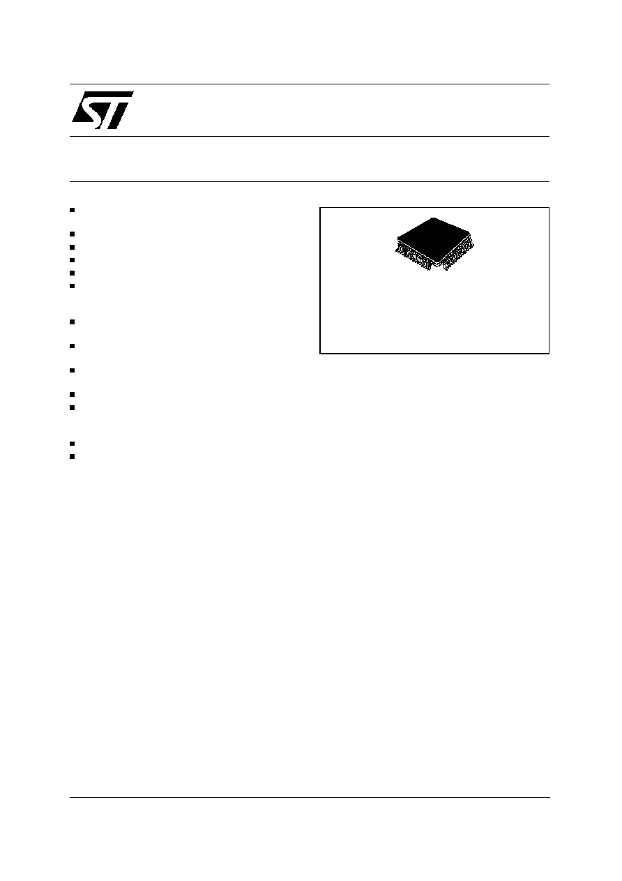
64 TQFP PACKAGE
PCM IN HI-Z MODE
DESCRIPTION
The STLC5046 is a monolithic programmable 4
channel codec and filter. It operates with a single
+3.3V supply. The analog interface is based on a
receive output buffer driving the SLIC RX input
and on an amplifier input stage. Due to the single
supply voltage a proper midsupply reference level
is generated internally by the device and all ana-
log signals are referred to this level (AGND). The
PCM interface uses one common 8KHz frame
sync. pulse for transmit and receive direction. The
bit clock can be selected between four standards:
1.536/1.544MHz,
2.048MHz,
4.096MHz,
8192MHz. Device programmability is achieved
by means of 41 registers allowing to set the dif-
ferent parameters like TX/RX gains, encoding law
(A/
Á
), time slot assignment, independent chan-
nels power up/down, loopbacks, PCM bits offset.
Thanks to pinstrap option, the most significant of
the above parameters can be set by hardware
connection of dedicated pins. This allow to use
this device also on line card without MCU on
board. When pin strap option is selected different
pins of the device will change their function (see
pin description).
In MCU control mode the STLC5046 can be pro-
grammed via serial interface running up to 4MHz.
One interrupt output pin is also provided.
This is preliminary information on a new product now in development. Details are subject to change without notice.
December 1999
«
TQFP64
ORDERING NUMBER: STLC5046
STLC5046
PROGRAMMABLE FOUR CHANNEL CODEC AND FILTER
PRODUCT PREVIEW
1/27

ABSOLUTE MAXIMUM RATINGS
Symbol
Parameter
Value
Unit
V
CC
V
CC
to V
EE
-0.5 to 4.6
V
V
DD
V
DD
to V
SS
-0.5 to 4.6
V
V
DI
Digital Input Input Pin Voltage
-0.5 to 5.5
V
I
OUT
Output Pin Current
▒
1
mA
T
STG
Storage Temperature Range
-65 to +150
░
C
T
LEAD
Lead Temperature (soldering, 10s)
300
░
C
V
AI
Analog Pin Input Voltage
-0.5 to 4.6
V
OPERATING RANGE
Symbol
Parameter
Value
Unit
V
CC
, V
DD
Supply Voltage
3.3
▒
5%
V
T
OP
Operating Temperature Range
-40 to +85
░
C
THERMAL DATA
Symbol
Parameter
Value
Unit
R
th j-amb
Thermal Resistance Junction-Ambient
70
░
C/W
GR0
GR0
GR0
GR0
D/A
sigma-delta
DECIMATORS
TX FILTERS
RX FILTERS
INTERPOLATORS
ARBITER
ENCODER
DECODER
PROGRAMMABLE
GAIN RX
PROGRAMMABLE
GAIN TX
VFRO0
VFRO1
VFRO2
VFRO3
VFXI0
VFXI1
VFXI2
VFXI3
FS/FS0
MCLK
TSX
DX
DR
SLIC
CONTROL
REGISTERS
8bit
8bit
17-bit
Bus
data
contlol
to analog FE
Post
Filter
Post
Post
Post
Filter
Filter
Filter
Programmable
functions
8-bit
Bus
A/D
A/D
A/D
A/D
Anti-Alias
Anti-Alias
Anti-Alias
Anti-Alias
GX0
GX1
GX2
GX3
A/u Law
A/u Law
PCM
INTERFACE
& SLOT ASSGN
DIGITAL PROCESSOR
ANALOG FRONTEND
VEE
VCC
PLL
INTERFACE
CONTROL
SERIAL
CS / PD1
CO / GR0
CI / PD0
CCLK / GR1
INT / AMU
CS0 / GX0
CS1 / GX1
CS2 / GX2
CS3 / GX3
IO0 / GR2
IO1 / PD2
IO2 / GR3
IO3 / PD3
IO7
IO8
IO9
IO10
IO11
CAP
VDD
VSS
SUB
CONFIG.
PORT
IO4 / FS1
IO5 / FS2
IO6 / FS3
M0
M1
BLOCK DIAGRAM
GR0
GR1
GR2
GR3
STLC5046
2/27

ANALOG
N.
Name
Type
Function
33
VFRO0
AO
Receive analog amplifier output channel 0. PCM data received on the programmed
Time Slot on DR input is decoded and appears at this output.
39
VFRO1
AO
Receive analog amplifier output channel 1. PCM data received on the programmed
Time Slot on DR input is decoded and appears at this output.
42
VFRO2
AO
Receive analog amplifier output channel 2. PCM data received on the programmed
Time Slot on DR input is decoded and appears at this output.
48
VFRO3
AO
Receive analog amplifier output channel 3. PCM data received on the programmed
Time Slot on DR input is decoded and appears at this output.
1
2
3
5
6
4
7
8
9
10
27
11
28 29 30 31 32
59 58 57 56
54
55
53 52 51 50 49
43
42
41
39
38
40
48
47
46
44
45
CI/PD0
CO/GR0
CS/PD1
RES
RES
INT/AMU
DX
DR
VDD
CCLK/GR1
VSS
IO3/PD3
IO4/FS1
IO5/FS2
VCC5
M0
VEE5
CS0/GX0
CS1/GX1
VEE1
VEE0
N.C.
IO9
IO10
IO11
VCC4
M1
VEE4
CS2/GX2
CS3/GX3
VEE2
VEE3
N.C.
VFXI2
VFRO2
SUB
VFRO1
VFXI1
CAP
VFRO3
N.C.
VFXI3
VCC2
VCC3
D98TL405
22 23 24 25 26
60
IO8
61
IO7
62
IO6/FS3
63
RES
64
N.C.
N.C.
N.C.
IO0/GR2
IO1/PD2
IO2/GR3
17 18 19 20 21
37
36
34
33
35
VCC1
VCC0
N.C.
VFRO0
VFXI0
12
13
14
15
16
N.C.
N.C.
FS/FS0
TSX
MCLK
PIN CONNECTION (Top view)
PIN DESCRIPTION
I/O DEFINITION
Type
Definition
AI
Analog Input
AO
Analog Output
ODO
Open Drain Output
DI
Digital Input
DO
Digital Output
DIO
Digital Input/Output
DTO
Digital Tristate Output
DPS
Digital Power Supply
APS
Analog Power Supply
STLC5046
3/27

N.
Name
Type
Function
35
VFXI0
AI
TX Input Amplifier channel 0. Typ 1M
input impedance
38
VFXI1
AI
TX Input Amplifier channel 1. Typ 1M
input impedance
43
VFXI2
AI
TX Input Amplifier channel 2. Typ 1M
input impedance
46
VFXI3
AI
TX Input Amplifier channel 3. Typ 1M
input impedance
40
CAP
AI
AGND Voltage filter pin. A 100nF capacitor must be connected between ground and
this pin.
POWER SUPPLY
25, 36,
37, 44,
45, 56,
VCC/0/1/2/3/
4/5
APS
Total 6 pins: 3.3V analog power supplies, should be shorted together, require 100nF
decoupling capacitor to VEE.
26,30,
31, 50,
51,55
VEE/0/1/2/3/
4/5
APS
Total 6 pins: analog ground, should be shorted together.
9
VDD
DPS
Digital Power supply 3.3V, require 100nF decoupling capacitor to VSS.
8
VSS
DPS
Digital Ground
41
SUB
DPS
Substrate connection. Must be shorted together with VEE and VSS pins as close as
possible the chip.
NOT CONNECTED
15, 16,
17, 18,
32, 34,
47, 49,
64
N.C.
Not Connected.
1,2,63
RES
Reserved: must be left not connected.
DIGITAL
27
M0
DI
Mode select, see M1
M1
M0
Mode Select
0
1
Pin-strap mode: Basic functions selected by proper pin strapping
1
0
MCU mode: Device controlled via serial interface
0
0
Reset status
1
1
Not Allowed
54
M1
DI
13
MCLK
DI
Master Clock Input.
Four possible frequencies can be used:
1.536/1.544 MHz; 2.048 MHz; 4.096 MHz; 8.192 MHz.
The device automatically detect the frequency applied.
This signal is also used as bit clock and it is used to shift data into and out of the DR
and DX pins.
12
TSX
ODO
Transmit Time Slot (open drain output, 3.2mA). Normally it is floating in high
impedance state except when a time slot is active on the DX output. In this case TSX
output pulls low to enable the backplane line driver.
11
DX
DTO
Transmit PCM interface. It remains in high impedance state except during the
assigned time slots during wich the PCM data byte is shifted out on the rising edge of
MCLK.
10
DR
DI
Receive PCM interface. It remains inactive except during the assigned receive time
slots during which the PCM data byte is shifted in on the falling edge of MCLK.
61
IO7
DIO
Slic control I/O pin #7. Can be programmed as input or output via DIR register.
Depending on content of CONF register can be a static input/output or a dynamic
input/output synchronized with the CSn output signals controlling the SLICs.
PIN DESCRIPTION (continued)
ANALOG
STLC5046
4/27

N.
Name
Type
Function
60
IO8
DIO
Slic control I/O pin #8. (see IO7 description).
59
IO9
DIO
Slic control I/O pin #9. (see IO7 description).
58
IO10
DIO
Slic control I/O pin #10. (see IO7 description).
57
IO11
DIO
Slic control I/O pin #11. (see IO7 description).
DIGITAL (DUAL MODE)
14
FS/FS0
DI
MCU control mode: FS.
Frame Sync. Pulse. A pulse or a squarewave waveform with an 8kHz repetition rate
is applied to this pin to define the start of the receive and transmit frame. Effective
start of the frame can be then shifted of up to 7 clock pulses indipendently in receive
and transmit directions by proper programming of the PCMSH register.
Pin-strap control mode: FS0.
Frame Sync. pulse of channel #0. One MCLK cycle long , starts PCM data transfer in
the Time Slot following its falling edge (Short Frame Delayed Timing).
19
IO0/GR2
DIO/DI
MCU control mode: IO0.
Slic control I/O pin #0. Can be programmed as input or output via DIR register.
Depending on content of CONF register can be a static input/output or a dynamic
input/output synchronized with the CSn output signals controlling the SLICs.
Pin-strap control mode: GR2.
Receive gain programming channel 2:
1: Receive gain = = -0.8dB
0: Rec. gain = -4.3dB
20
IO1/PD2
DIO/DI
MCU control mode: IO1.
Slic control I/O pin #1. (see IO0 description).
Pin-strap control mode: PD2.
Power Down command channel 2:
1: Channel 2 Codec is in power down.
(equivalent to CONF reg bit2 = 1)
0: Channel 2 Codec is in power up.
(equivalent to CONF reg. bit2 = 0)
21
IO2/GR3
DIO/DI
MCU control mode: IO2.
Slic control I/O pin #2. (see IO0 description)
Pin-strap control mode: GR3.
Receive gain programming channel 3. (see GR2 description)
22
IO3/PD3
DIO/DI
MCU control mode: IO3.
Slic control I/O pin #3. (see IO0 description).
Pin-strap control mode: PD3.
Power Down command channel 3. (see PD2 description)
23
IO4/FS1
DIO/DI
MCU control mode: IO4
Slic control I/O pin #4. (see IO0 description).
Pin-strap control mode: FS1.
Frame Sync. pulse of channel #1. One MCLK cycle long , starts PCM data transfer in
the Time Slot following its falling edge (Short Frame Delayed Timing).
24
IO5/FS2
DIO/DI
MCU control mode: IO4.
Slic control I/O pin #5. (see IO0 description).
Pin-strap control mode: FS2.
Frame Sync. pulse of channel #1. One MCLK cycle long , starts PCM data transfer in
the Time Slot following its falling edge (Short Frame Delayed Timing).
62
IO6/FS3
DIO/DI
MCU control mode: IO4.
Slic control I/O pin #6. (see IO0 description).
Pin-strap control mode: FS3.
Frame Sync. pulse of channel #1. One MCLK cycle long , starts PCM data transfer in
the Time Slot following its falling edge (Short Frame Delayed Timing).
PIN DESCRIPTION (continued)
DIGITAL
STLC5046
5/27


