
STH6N100
STH6N100FI
N - CHANNEL ENHANCEMENT MODE
POWER MOS TRANSISTOR
s
TYPICAL R
DS(on)
= 1.75
s
AVALANCHE RUGGED TECHNOLOGY
s
100% AVALANCHE TESTED
s
REPETITIVE AVALANCHE DATA AT 100
o
C
s
LOW INPUT CAPACITANCE
s
LOW GATE CHARGE
s
APPLICATION ORIENTED
CHARACTERIZATION
APPLICATIONS
s
HIGH CURRENT, HIGH SPEED SWITCHING
s
SWITCH MODE POWER SUPPLIES (SMPS)
s
CONSUMER AND INDUSTRIAL LIGHTING
s
DC-AC INVERTERS FOR WELDING
EQUIPMENT AND UNINTERRUPTIBLE
POWER SUPPLY (UPS)
INTERNAL SCHEMATIC DIAGRAM
TYPE
V
DSS
R
DS ( on)
I
D
STH6N100
STH6N100FI
1000 V
1000 V
< 2
< 2
6 A
3.7 A
1
2
3
TO-218
ISOWATT218
December 1996
ABSOLUTE MAXIMUM RATINGS
Symbol
Parameter
Val ue
Unit
STH6N100
STH6N100
V
D S
Drain-source Voltage (V
GS
= 0)
1000
V
V
DG R
Drain- gate Voltage (R
GS
= 20 k
)
1000
V
V
GS
Gate-source Voltage
±
20
V
I
D
Drain Current (cont inuous) at T
c
= 25
o
C
6
3.7
A
I
D
Drain Current (cont inuous) at T
c
= 100
o
C
3.7
2.3
A
I
D M
(
·
)
Drain Current (pulsed)
24
24
A
P
tot
Total Dissipation at T
c
= 25
o
C
180
70
W
Derating Factor
1. 44
0.56
W/
o
C
V
ISO
I nsulat ion Withstand Voltage (DC)
4000
V
T
stg
St orage Temperat ure
-65 to 150
o
C
T
j
Max. Operat ing Junction Temperature
150
o
C
(
·
) Pulse width limited by safe operating area
1
2
3
1/10
THERMAL DATA
TO-218
ISOWATT218
R
thj-cas e
Thermal Resist ance Junct ion-case
Max
0.69
1. 78
o
C/W
R
thj- amb
R
t hc- sin k
T
l
Thermal Resist ance Junct ion-ambient
Max
Thermal Resist ance Case-sink
Typ
Maximum Lead Temperature For Soldering Purpose
30
0.1
300
o
C/W
o
C/W
o
C
AVALANCHE CHARACTERISTICS
Symbol
Parameter
Max Value
Uni t
I
A R
Avalanche Current, Repetitive or Not-Repetitive
(pulse width limited by T
j
max,
< 1%)
6
A
E
AS
Single Pulse Avalanche Energy
(st arting T
j
= 25
o
C, I
D
= I
AR
, V
D D
= 25 V)
850
mJ
E
AR
Repet itive Avalanche Energy
(pulse width limited by T
j
max,
< 1%)
16
mJ
I
A R
Avalanche Current, Repetitive or Not-Repetitive
(T
c
= 100
o
C, pulse width limited by T
j
max,
< 1%)
3.7
A
ELECTRICAL CHARACTERISTICS (T
case
= 25
o
C unless otherwise specified)
OFF
Symbol
Parameter
Test Condi tions
Mi n.
Typ.
Max.
Unit
V
( BR)DSS
Drain-source
Breakdown Voltage
I
D
= 250
µ
A
V
G S
= 0
1000
V
I
DS S
Zero Gate Volt age
Drain Current (V
GS
= 0)
V
DS
= Max Rating
V
DS
= Max Rating x 0.8
T
c
= 125
o
C
25
250
µ
A
µ
A
I
G SS
Gate-body Leakage
Current (V
D S
= 0)
V
GS
=
±
20 V
±
100
nA
ON (
)
Symbol
Parameter
Test Condi tions
Mi n.
Typ.
Max.
Unit
V
G S(th)
Gate Threshold Voltage V
DS
= V
GS
I
D
= 250
µ
A
2
3
4
V
R
DS( on)
St atic Drain-source On
Resist ance
V
GS
= 10V
I
D
= 3 A
1.75
2
I
D( on)
On St ate Drain Current
V
DS
> I
D( on)
x R
D S(on) max
V
GS
= 10 V
6
A
DYNAMIC
Symbol
Parameter
Test Condi tions
Mi n.
Typ.
Max.
Unit
g
fs
(
)
Forward
Transconductance
V
DS
> I
D( on)
x R
D S(on) max
I
D
= 3 A
4
5.5
S
C
iss
C
oss
C
rss
I nput Capacitance
Output Capacit ance
Reverse Transfer
Capacitance
V
DS
= 25 V
f = 1 MHz
V
G S
= 0
2150
260
105
2800
330
130
pF
pF
pF
STH6N100/FI
2/10
ELECTRICAL CHARACTERISTICS (continued)
SWITCHING ON
Symbol
Parameter
Test Condi tions
Mi n.
Typ.
Max.
Unit
t
d(on)
t
r
Turn-on Time
Rise Time
V
DD
= 500 V
I
D
= 3 A
R
G
= 50
V
GS
= 10 V
(see test circuit, figure 3)
70
210
90
280
ns
ns
(di/dt)
on
Turn-on Current Slope
V
DD
= 800 V
I
D
= 6 A
R
G
= 50
V
GS
= 10 V
(see test circuit, figure 5)
180
A/
µ
s
Q
g
Q
gs
Q
gd
Total Gate Charge
Gate-Source Charge
Gate-Drain Charge
V
DD
= 400 V
I
D
= 6 A
V
GS
= 10 V
125
15
55
150
nC
nC
nC
SWITCHING OFF
Symbol
Parameter
Test Condi tions
Mi n.
Typ.
Max.
Unit
t
r(Vof f)
t
f
t
c
Of f-voltage Rise Time
Fall Time
Cross-over Time
V
DD
= 800 V
I
D
= 6 A
R
G
= 50
V
GS
= 10 V
(see test circuit, figure 5)
190
50
265
250
65
345
ns
ns
ns
SOURCE DRAIN DIODE
Symbol
Parameter
Test Condi tions
Mi n.
Typ.
Max.
Unit
I
S D
I
SD M
(
·
)
Source-drain Current
Source-drain Current
(pulsed)
6
24
A
A
V
S D
(
)
Forward On Volt age
I
SD
= 6 A
V
GS
= 0
2
V
t
rr
Q
rr
I
RRM
Reverse Recovery
Time
Reverse Recovery
Charge
Reverse Recovery
Current
I
SD
= 6 A
di/dt = 100 A/
µ
s
V
DD
= 100 V
T
j
= 150
o
C
(see test circuit, figure 5)
1100
31
57
ns
µ
C
A
(
) Pulsed: Pulse duration = 300
µ
s, duty cycle 1.5 %
(
·
) Pulse width limited by safe operating area
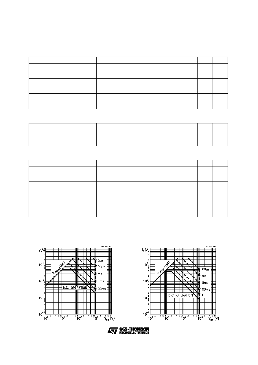
Safe Operating Areas For TO-218
Safe Operating Areas For ISOWATT218
STH6N100/FI
3/10

Thermal Impedeance For TO-218
Derating Curve For TO-218
Output Characteristics
Thermal Impedance For ISOWATT218
Derating Curve For ISOWATT218
Transfer Characteristics
STH6N100/FI
4/10
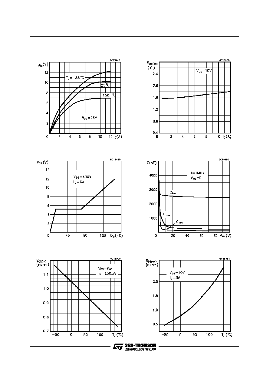
Transconductance
Static Drain-source On Resistance
Gate Charge vs Gate-source Voltage
Capacitance Variations
Normalized On Resistance vs Temperature
Normalized Gate Threshold Voltage vs
Temperature
STH6N100/FI
5/10
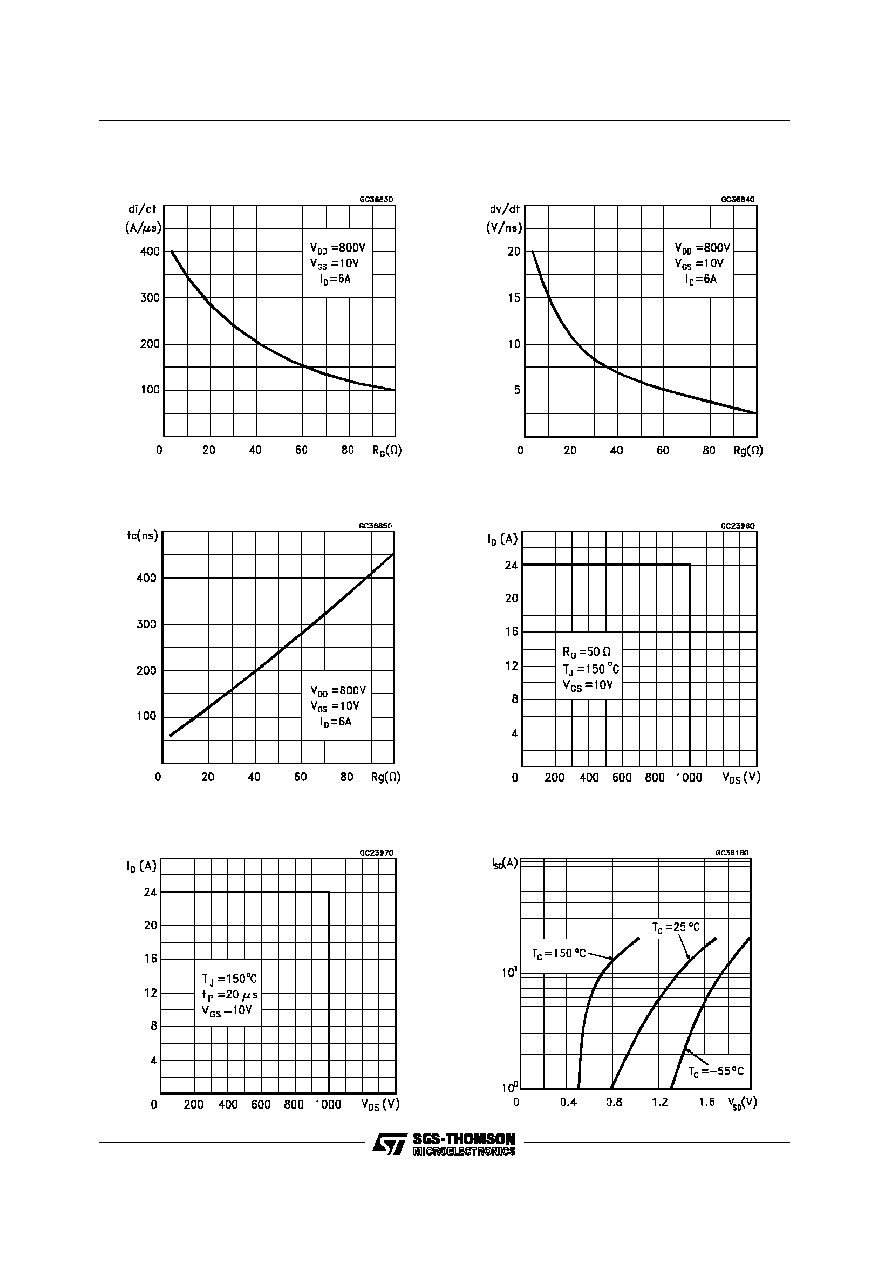
Turn-on Current Slope
Turn-off Drain-source Voltage Slope
Cross-over Time
Switching Safe Operating Area
Accidental Overload Area
Source-drain Diode Forward Characteristics
STH6N100/FI
6/10

Fig. 2: Unclamped Inductive Waveforms
Fig. 3: Switching Times Test Circuits For
Resistive Load
Fig. 4: Gate Charge Test Circuit
Fig. 5: Test Circuit For Inductive Load Switching
And Diode Reverse Recovery Time
Fig. 1: Unclamped Inductive Load Test Circuits
STH6N100/FI
7/10
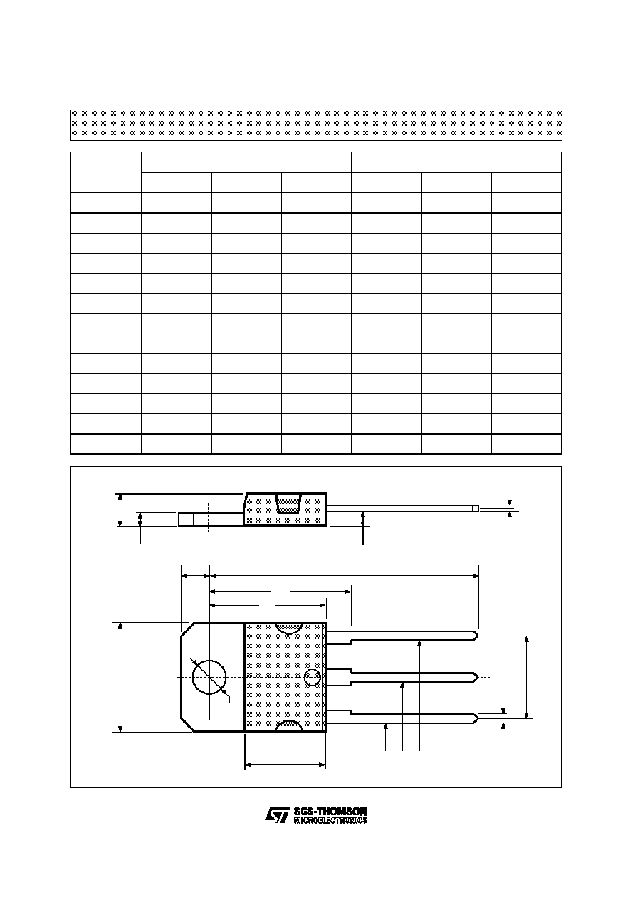
DIM.
mm
inch
MIN.
TYP.
MAX.
MIN.
TYP.
MAX.
A
4.7
4.9
0.185
0.193
C
1.17
1.37
0.046
0.054
D
2.5
0.098
E
0.5
0.78
0.019
0.030
F
1.1
1.3
0.043
0.051
G
10.8
11.1
0.425
0.437
H
14.7
15.2
0.578
0.598
L2
16.2
0.637
L3
18
0.708
L5
3.95
4.15
0.155
0.163
L6
31
1.220
R
12.2
0.480
Ř
4
4.1
0.157
0.161
R
A
C
D
E
H
F
G
L6
Ř
L3
L2
L5
1
2
3
TO-218 (SOT-93) MECHANICAL DATA
P025A
STH6N100/FI
8/10
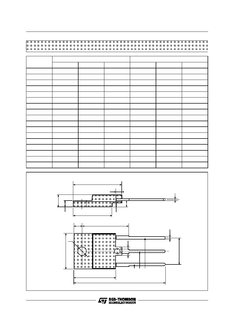
DIM.
mm
inch
MIN.
TYP.
MAX.
MIN.
TYP.
MAX.
A
5.35
5.65
0.210
0.222
C
3.3
3.8
0.130
0.149
D
2.9
3.1
0.114
0.122
D1
1.88
2.08
0.074
0.081
E
0.45
1
0.017
0.039
F
1.05
1.25
0.041
0.049
G
10.8
11.2
0.425
0.441
H
15.8
16.2
0.622
0.637
L1
20.8
21.2
0.818
0.834
L2
19.1
19.9
0.752
0.783
L3
22.8
23.6
0.897
0.929
L4
40.5
42.5
1.594
1.673
L5
4.85
5.25
0.190
0.206
L6
20.25
20.75
0.797
0.817
M
3.5
3.7
0.137
0.145
N
2.1
2.3
0.082
0.090
U
4.6
0.181
L1
A
C
D
E
H
G
M
F
L6
1
2
3
U
L5
L4
D1
N
L3
L2
ISOWATT218 MECHANICAL DATA
P025C
STH6N100/FI
9/10

Information furnished is believed to be accurate and reliable. However, SGS-THOMSON Microelectronics assumes no responsability for the
consequences of use of such information nor for any infringement of patents or other rights of third parties which may results from its use. No
license is granted by implication or otherwise under any patent or patent rights of SGS-THOMSON Microelectronics. Specifications mentioned
in this publication are subject to change without notice. This publication supersedes and replaces all information previously supplied.
SGS-THOMSON Microelectronics products are not authorized for use as critical components in life support devices or systems without express
written approval of SGS-THOMSON Microelectonics.
©
1996 SGS-THOMSON Microelectronics - Printed in Italy - All Rights Reserved
SGS-THOMSON Microelectronics GROUP OF COMPANIES
Australia - Brazil - Canada - China - France - Germany - Hong Kong - Italy - Japan - Korea - Malaysia - Malta - Morocco - The Netherlands -
Singapore - Spain - Sweden - Switzerland - Taiwan - Thailand - United Kingdom - U.S.A
.
STH6N100/FI
10/10