
STF2222A
SMALL SIGNAL NPN TRANSISTOR
PRELIMINARY DATA
s
SILICON EPITAXIAL PLANAR NPN
TRANSISTOR
s
MINIATURE SOT-89 PLASTIC PACKAGE
FOR SURFACE MOUNTING CIRCUITS
s
TAPE & REEL PACKING
s
THE PNP COMPLEMENTARY TYPE IS
STF2907A
APPLICATIONS
s
WELL SUITABLE FOR PORTABLE
EQUIPMENT
s
SMALL LOAD SWITCH TRANSISTOR WITH
HIGH GAIN AND LOW SATURATION
VOLTAGE
INTERNAL SCHEMATIC DIAGRAM
February 2003
Type
Marking
STF2222A
20F
ABSOLUTE MAXIMUM RATINGS
Symbol
Parameter
Value
Unit
V
CBO
Collector-Emitter Voltage (I
E
= 0)
75
V
V
CEO
Collector-Emitter Voltage (I
B
= 0)
40
V
V
EBO
Emitter-Base Voltage (I
C
= 0)
6
V
I
C
Collector Current
0.6
A
I
CM
Collector Peak Current (t
p
< 5 ms)
0.8
A
P
tot
Total Dissipation at T
amb
= 25
o
C
1.2
W
T
stg
Storage Temperature
-65 to 150
o
C
T
j
Max. Operating Junction Temperature
150
o
C
®
SOT-89
1/5

THERMAL DATA
R
thj-amb
·
Thermal Resistance Junction-Ambient Max
104.1
o
C/W
·
Device mounted on a PCB area of 1 cm
2
.
ELECTRICAL CHARACTERISTICS (T
case
= 25
o
C unless otherwise specified)
Symbol
Parameter
Test Conditions
Min.
Typ.
Max.
Unit
I
CEX
Collector Cut-off
Current (V
BE
= -3 V)
V
CE
= 60 V
10
nA
I
BEX
Base Cut-off Current
(V
BE
= -3 V)
V
CE
= 60 V
20
nA
I
CBO
Collector Cut-off
Current (I
E
= 0)
V
CB
= 75 V
V
CB
= 75 V T
j
= 150
o
C
10
10
nA
µ
A
I
EBO
Emitter Cut-off Current
(I
C
= 0)
V
EB
= 3 V
15
nA
V
(BR)CEO
Collector-Emitter
Breakdown Voltage
(I
B
= 0)
I
C
= 10 mA
40
V
V
(BR)CBO
Collector-Base
Breakdown Voltage
(I
E
= 0)
I
C
= 10
µ
A
75
V
V
(BR)EBO
Emitter-Base
Breakdown Voltage
(I
C
= 0)
I
E
= 10
µ
A
6
V
V
CE(sat)
Collector-Emitter
Saturation Voltage
I
C
= 150 mA I
B
= 15 mA
I
C
= 500 mA I
B
= 50 mA
0.3
1
V
V
V
BE(sat)
Collector-Base
Saturation Voltage
I
C
= 150 mA I
B
= 15 mA
I
C
= 500 mA I
B
= 50 mA
0.6
1.2
2
V
V
h
FE
DC Current Gain
I
C
= 0.1 mA V
CE
= 10 V
I
C
= 1 mA V
CE
= 10 V
I
C
= 10 mA V
CE
= 10 V
I
C
= 150 mA V
CE
= 10 V
I
C
= 150 mA V
CE
= 1 V
I
C
= 500 mA V
CE
= 10 V
35
50
75
100
50
40
300
f
T
Transition Frequency
I
C
= 20 mA V
CE
= 20V f = 100MHz
270
MHz
C
CBO
Collector-Base
Capacitance
I
E
= 0 V
CB
= 10 V f = 1 MHz
4
8
pF
C
EBO
Emitter-Base
Capacitance
I
C
= 0 V
EB
= 0.5 V f = 1MHz
20
25
pF
NF
Noise Figure
I
C
= 0.1 mA V
CE
= 10 V f = 1 KHz
f = 200 Hz R
G
= 1 K
4
dB
h
ie
Input Impedance
V
CE
= 10 V I
C
= 1 mA f = 1 KHz
V
CE
= 10 V I
C
= 10 mA f = 1 KHz
2
0.25
8
1.25
K
K
h
re
Reverse Voltage Ratio
V
CE
= 10 V I
C
= 1 mA f = 1 KHz
V
CE
= 10 V I
C
= 10 mA f = 1 KHz
8
4
10
-4
10
-4
h
fe
Small Signal Current
Gain
V
CE
= 10 V I
C
= 1 mA f = 1 KHz
V
CE
= 10 V I
C
= 10 mA f = 1 KHz
50
75
300
375
h
oe
Output Admittance
V
CE
= 10 V I
C
= 1 mA f = 1 KHz
V
CE
= 10 V I
C
= 10 mA f = 1 KHz
5
25
35
200
µ
S
µ
S
Pulsed: Pulse duration = 300
µ
s, duty cycle
2 %
STF2222A
2/5

ELECTRICAL CHARACTERISTICS (Continued)
Symbol
Parameter
Test Conditions
Min.
Typ.
Max.
Unit
t
d
Delay Time
I
C
= 150 mA I
B
= 15 mA
V
CC
= 30 V
5
10
ns
t
r
Rise Time
12
25
ns
t
s
Storage Time
I
C
= 150 mA I
B1
= - I
B2
= 15 mA
V
CC
= 30 V
185
225
ns
t
f
Fall Time
24
60
ns
Pulsed: Pulse duration = 300
µ
s, duty cycle
2 %
STF2222A
3/5
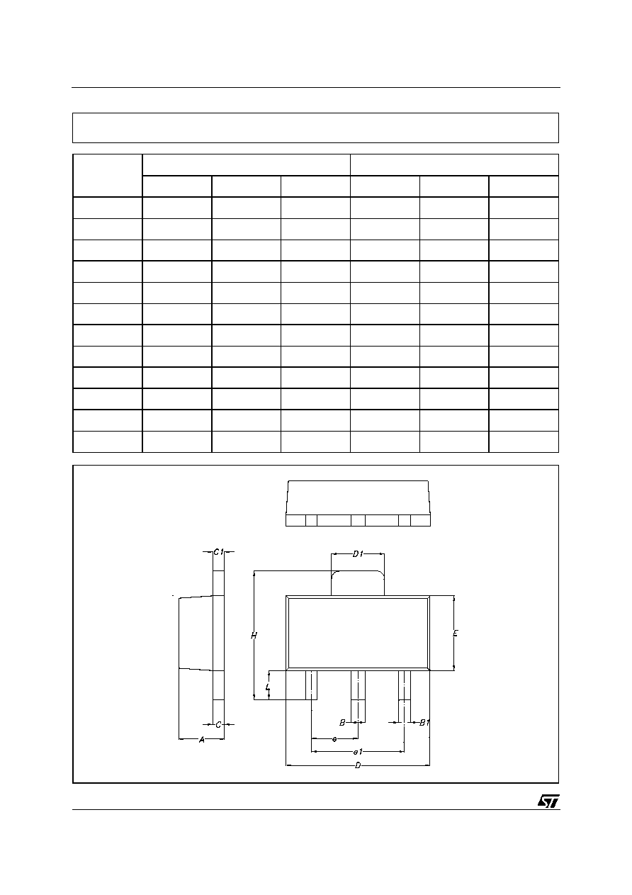
DIM.
mm
mils
MIN.
TYP.
MAX.
MIN.
TYP.
MAX.
A
1.4
1.6
55.1
63.0
B
0.44
0.56
17.3
22.0
B1
0.36
0.48
14.2
18.9
C
0.35
0.44
13.8
17.3
C1
0.35
0.44
13.8
17.3
D
4.4
4.6
173.2
181.1
D1
1.62
1.83
63.8
72.0
E
2.29
2.6
90.2
102.4
e
1.42
1.57
55.9
61.8
e1
2.92
3.07
115.0
120.9
H
3.94
4.25
155.1
167.3
L
0.89
1.2
35.0
47.2
P025H
SOT-89 MECHANICAL DATA
STF2222A
4/5
Information furnished is believed to be accurate and reliable. However, STMicroelectronics assumes no responsibility for the consequences
of use of such information nor for any infringement of patents or other rights of third parties which may result from its use. No license is
granted by implication or otherwise under any patent or patent rights of STMicroelectronics. Specification mentioned in this publication are
subject to change without notice. This publication supersedes and replaces all information previously supplied. STMicroelectronics products
are not authorized for use as critical components in life support devices or systems without express written approval of STMicroelectronics.
The ST logo is a trademark of STMicroelectronics
© 2003 STMicroelectronics Printed in Italy All Rights Reserved
STMicroelectronics GROUP OF COMPANIES
Australia - Brazil - Canada - China - Finland - France - Germany - Hong Kong - India - Israel - Italy - Japan - Malaysia - Malta - Morocco -
Singapore - Spain - Sweden - Switzerland - United Kingdom - United States.
http://www.st.com
STF2222A
5/5