
1/8
September 2001
.
STE250NS10
N-CHANNEL 100V - 0.0045
- 220A ISOTOP
STripFETTM POWER MOSFET
s
TYPICAL R
DS
(on) = 0.0045
s
STANDARD THRESHOLD DRIVE
s
100% AVALANCHE TESTED
APPLICATIONS
s
SMPS & UPS
s
MOTOR CONTROL
s
WELDING EQUIPMENT
s
OUTPUT STAGE FOR PWM, ULTRASONIC
CIRCUITS
TYPE
V
DSS
R
DS(on)
I
D
STE250NS10
100 V
<0.0055
220A
ABSOLUTE MAXIMUM RATINGS
(
·)
Pulse width limited by safe operating area.
(1 )I
SD
220A, di/dt
200A/µs, V
DD
V
(BR)DSS
, T
j
T
JMAX
.
Symbol
Parameter
Value
Unit
V
DS
Drain-source Voltage (V
GS
= 0)
100
V
V
DGR
Drain-gate Voltage (R
GS
= 20 k
)
100
V
V
GS
Gate- source Voltage
± 20
V
I
D
Drain Current (continuos) at T
C
= 25°C
220
A
I
D
Drain Current (continuos) at T
C
= 100°C
156
A
I
DM
(
·)
Drain Current (pulsed)
880
A
P
tot
Total Dissipation at T
C
= 25°C
500
W
Derating Factor
4
W/°C
dv/dt
(1)
Peak Diode Recovery voltage slope
3.5
V/ns
V
ISO
Insulation Withstand Voltage (AC-RMS)
2500
V
T
stg
Storage Temperature
-55 to 150
°C
T
j
Operating Junction Temperature
150
°C
ISOTOP
INTERNAL SCHEMATIC DIAGRAM

STE250NS10
2/8
THERMAL DATA
AVALANCHE CHARACTERISTICS
ELECTRICAL CHARACTERISTICS (T
case
= 25 °C unless otherwise specified)
OFF
ON
(*)
DYNAMIC
Rthj-case
Rthj-amb
Thermal Resistance Junction-case
Thermal Resistance Junction-ambient
Max
Max
0.25
50
°C/W
°C/W
Symbol
Parameter
Max Value
Unit
I
AR
Avalanche Current, Repetitive or Not-Repetitive
(pulse width limited by T
j
max)
220
A
E
AS
Single Pulse Avalanche Energy
(starting T
j
= 25 °C, I
D
= I
AR
, V
DD
= 64 V)
800
mJ
Symbol
Parameter
Test Conditions
Min.
Typ.
Max.
Unit
V
(BR)DSS
Drain-source Breakdown
Voltage
I
D
= 1 mA
V
GS
= 0
100
V
I
DSS
Zero Gate Voltage
Drain Current (V
GS
= 0)
V
DS
= Max Rating
V
DS
= Max Rating T
C
= 125°C
50
500
µA
µA
I
GSS
Gate-body Leakage
Current (V
DS
= 0)
V
GS
= ± 20V
±400
nA
Symbol
Parameter
Test Conditions
Min.
Typ.
Max.
Unit
V
GS(th)
Gate Threshold Voltage
V
DS
= V
GS
I
D
= 250 µA
2
3
4
V
R
DS(on)
Static Drain-source On
Resistance
V
GS
= 10 V
I
D
= 125 A
0.0045
0.0055
Symbol
Parameter
Test Conditions
Min.
Typ.
Max.
Unit
g
fs
Forward Transconductance
V
DS
= 20 V
I
D
= 70 A
60
S
C
iss
C
oss
C
rss
Input Capacitance
Output Capacitance
Reverse Transfer
Capacitance
V
DS
= 25V, f = 1 MHz, V
GS
= 0
31
4.3
1.2
nF
nF
nF

3/8
STE250NS10
SWITCHING ON
SWITCHING OFF
SOURCE DRAIN DIODE
(*)
Pulsed: Pulse duration = 300 µs, duty cycle 1.5 %.
(
·)
Pulse width limited by safe operating area.
Symbol
Parameter
Test Conditions
Min.
Typ.
Max.
Unit
t
d(on)
t
r
Turn-on Delay Time
Rise Time
V
DD
= 50 V
I
D
= 125 A
R
G
= 4.7
V
GS
= 10 V
(Resistive Load, Figure 3)
110
380
ns
ns
Q
g
Q
gs
Q
gd
Total Gate Charge
Gate-Source Charge
Gate-Drain Charge
V
DD
= 50V I
D
= 220A V
GS
= 10V
900
160
330
nC
nC
nC
Symbol
Parameter
Test Conditions
Min.
Typ.
Max.
Unit
t
d(off)
t
f
Turn-off Delay Time
Fall Time
V
DD
= 50 V
I
D
= 125 A
R
G
= 4.7
,
V
GS
= 10 V
(Resistive Load, Figure 3)
1100
330
ns
ns
t
r(Voff)
t
f
t
c
Off-voltage Rise Time
Fall Time
Cross-over Time
V
clamp
= 80 V
I
D
= 220 A
R
G
= 4.7
,
V
GS
= 10 V
(Inductive Load, Figure 5)
950
330
600
ns
ns
ns
Symbol
Parameter
Test Conditions
Min.
Typ.
Max.
Unit
I
SD
I
SDM
(
·
)
Source-drain Current
Source-drain Current (pulsed)
220
880
A
A
V
SD
(*)
Forward On Voltage
I
SD
= 220 A
V
GS
= 0
1.5
V
t
rr
Q
rr
I
RRM
Reverse Recovery Time
Reverse Recovery Charge
Reverse Recovery Current
I
SD
= 220 A
di/dt = 100A/µs
V
DD
= 30 V
T
j
= 150°C
(see test circuit, Figure 5)
200
1.35
13.5
ns
µ
C
A
ELECTRICAL CHARACTERISTICS (continued)
Safe Operating Area
Thermal Impedance
STE250NS10
4/8
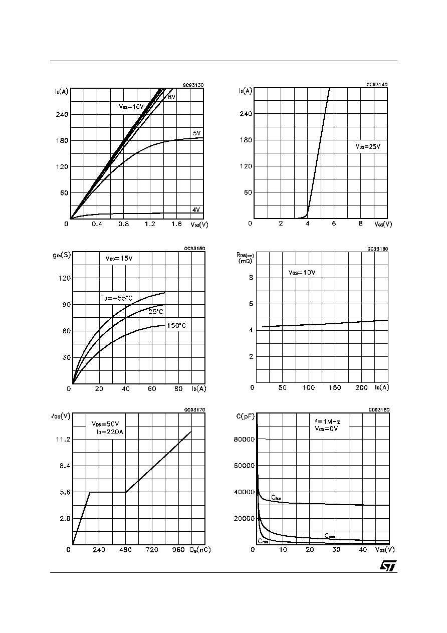
Output Characteristics
Transfer Characteristics
Transconductance
Static Drain-source On Resistance
Gate Charge vs Gate-source Voltage
Capacitance Variations

5/8
STE250NS10
.
.
Normalized Gate Threshold Voltage vs Temperature
Normalized on Resistance vs Temperature
Source-drain Diode Forward Characteristics
Normalized Breakdown Voltage vs Temperature.
.
.

STE250NS10
6/8
Fig. 1: Unclamped Inductive Load Test Circuit
Fig. 1: Unclamped Inductive Load Test Circuit
Fig. 2: Unclamped Inductive Waveform
Fig. 3: Switching Times Test Circuits For Resistive
Load
Fig. 4: Gate Charge test Circuit
Fig. 5: Test Circuit For Inductive Load Switching
And Diode Recovery Times

7/8
STE250NS10
DIM.
mm
inch
MIN.
TYP.
MAX.
MIN.
TYP.
MAX.
A
11.8
12.2
0.466
0.480
B
8.9
9.1
0.350
0.358
C
1.95
2.05
0.076
0.080
D
0.75
0.85
0.029
0.033
E
12.6
12.8
0.496
0.503
F
25.15
25.5
0.990
1.003
G
31.5
31.7
1.240
1.248
H
4
0.157
J
4.1
4.3
0.161
0.169
K
14.9
15.1
0.586
0.594
L
30.1
30.3
1.185
1.193
M
37.8
38.2
1.488
1.503
N
4
0.157
O
7.8
8.2
0.307
0.322
B
E
H
O
N
J
K
L
M
F
A
C
G
D
ISOTOP MECHANICAL DATA

STE250NS10
8/8
Information furnished is believed to be accurate and reliable. However, STMicroelectronics assumes no responsibility for the consequences
of use of such information nor for any infringement of patents or other rights of third parties which may result from its use. No license is granted
by implication or otherwise under any patent or patent rights of STMicroelectronics. Specifications mentioned in this publication are subject
to change without notice. This publication supersedes and replaces all information previously supplied. STMicroelectronics products are not
authorized for use as critical components in life support devices or systems without express written approval of STMicroelectronics.
The ST logo is registered trademark of STMicroelectronics
®
2001 STMicroelectronics - All Rights Reserved
All other names are the property of their respective owners.
STMicroelectronics GROUP OF COMPANIES
Australia - Brazil - China - Finland - France - Germany - Hong Kong - India - Italy - Japan - Malaysia - Malta - Morocco -
Singapore - Spain - Sweden - Switzerland - United Kingdom - U.S.A.
http://www.st.com