Rev 3
December 2005
1/14
14
STP95N04
STD95N04
N-CHANNEL 40V - 5.4m
- 80A - DPAK - TO-220
STripFETTM Power MOSFET
General features
STANDARD THRESHOLD DRIVE
100% AVALANCHE TESTED
Description
This N-Channel enhancement mode MOSFET is
the latest refinement of STMicroelectronic unique
"Single Feature SizeTM" strip-based process with
less critical aligment steps and therefore a
remarkable manufacturing reproducibility. The
resulting transistor shows extremely high packing
density for low on-resistance, rugged avalanche
characteristics and low gate charge
.
Applications
HIGH CURRENT,SWITCHING APPLICATION
AUTOMOTIVE
Order codes
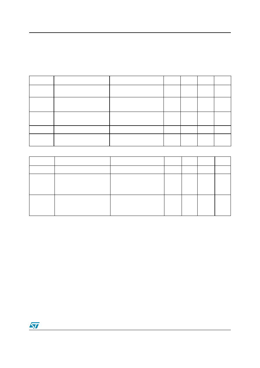
Internal schematic diagram
Type
V
DSS
R
DS(on)
I
D
Pw
STD95N04
STP95N04
40V
40V
<6.5m
<6.5m
80A
80A
110W
110W
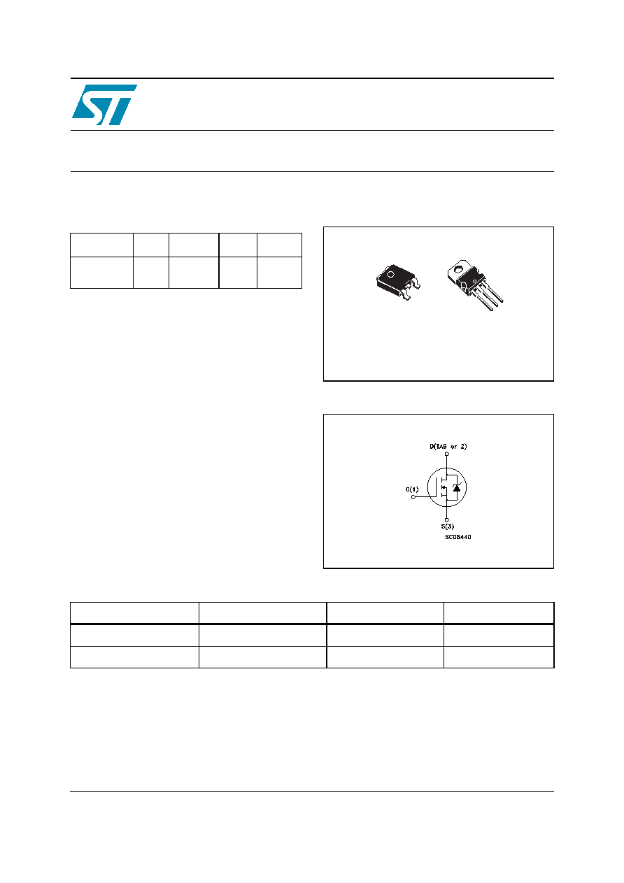
DPAK
1
3
1
2
3
TO-220
Sales Type
Marking
Package
Packaging
STD95N04
D95N04
DPAK
TAPE & REEL
STP95N04
P95N04
TO-220
TUBE
www.st.com

1 Electrical ratings
STD95N04 - STP95N04
2/14
1 Electrical
ratings
Table 1.
Absolute maximum ratings
Table 2.
Thermal data
Symbol
Parameter
Value
Unit
V
DS
Drain-source Voltage (V
GS
=0)
40
V
V
GS
Gate-Source Voltage
± 20
V
I
D
Note
1
Drain Current (continuous) at T
C
= 25°C
80
A
I
D
Drain Current (continuous) at T
C
= 100°C
65
A
I
DM
Note
2
Drain Current (pulsed)
320
A
P
TOT
Total Dissipation at T
C
= 25°C
110
W
Derating Factor
0.73
W/°C
dv/dt
Note
3 Peak Diode Recovery voltage slope
8
V/ns
E
AS
Note
4
Single Pulse Avalanche Energy
400
mJ
T
j
T
stg
Operating Junction Temperature
Storage Temperature
-55 to 175
°C
TO-220
DPAK
Rthj-case
Thermal Resistance Junction-case Max
1.36
°C/W
Rthj-a
Thermal Resistance Junction-ambient Max
62.5
--
°C/W
Rthj-pcb
Note
5
Thermal Resistance Junction-ambient Max
--
50
°C/W
T
l
Maximum Lead Temperature For Soldering
Purpose
300
--
°C
STD95N04 - STP95N04
2 Electrical characteristics
3/14
2 Electrical
characteristics
(T
CASE
= 25 °C unless otherwise specified)
Table 3.
On/off states
Table 4.
Dynamic
Symbol
Parameter
Test Conditions
Min.
Typ.
Max.
Unit
V
(BR)DSS
Drain-Source Breakdown
Voltage
I
D
= 250µA, V
GS
= 0
40
V
I
DSS
Zero Gate Voltage Drain
Current (V
GS
= 0)
V
DS
= Max Rating,
V
DS
= Max Rating,Tc = 125°C
10
100
µA
µA
I
GSS
Gate Body Leakage Current
(V
DS
= 0)
V
GS
= ±20V
±
200
nA
V
GS(th)
Gate Threshold Voltage
V
DS
= V
GS
, I
D
= 250µA
2
4
V
R
DS(on)
Static Drain-Source On
Resistance
V
GS
= 10V, I
D
= 40A
5.4
6.5
m
Symbol
Parameter
Test Conditions
Min.
Typ.
Max.
Unit
g
fs
Note
6
Forward Transconductance
V
DS
=25V, I
D
=40A
100
S
C
iss
C
oss
C
rss
Input Capacitance
Output Capacitance
Reverse Transfer Capacitance
V
DS
=25V, f=1 MHz, V
GS
=0
2200
580
40
pF
pF
pF
Q
g
Q
gs
Q
gd
Total Gate Charge
Gate-Source Charge
Gate-Drain Charge
V
DD
=20V, I
D
= 80A
V
GS
=10V
(see Figure 13)
40
11
8
54
nC
nC
nC
2 Electrical characteristics
STD95N04 - STP95N04
4/14
Table 5.
Switching times
Table 6.
Source drain diode
(1) Current limited by package
(2) Pulse width limited by safe operating area
(3) I
SD
80 A, di/dt
400A/µs, V
DS
V
(BR)DSS,
Tj
Tjmax
(4) Starting Tj=25°C, Id =40A, Vdd=30V
(5) When mounted on 1inch˛ FR4 2Oz Cu board
(6)Pulsed: pulse duration = 300µs, duty cycle 1.5%
Symbol
Parameter
Test Conditions
Min.
Typ.
Max.
Unit
t
d(on)
t
r
Turn-on Delay Time
Rise Time
V
DD
=20V, I
D
= 40A,
R
G
=4.7
,
V
GS
=10V
(see Figure 12)
15
50
ns
ns
t
d(off)
t
f
Turn-off Delay Time
FallTime
V
DD
=20V, I
D
= 40A,
R
G
=4.7
,
V
GS
=10V
(see Figure 12)
40
15
ns
ns
Symbol
Parameter
Test Conditions
Min.
Typ.
Max.
Unit
I
SD
I
SDM
Note
2
Source-drain Current
Source-drain Current (pulsed)
80
320
A
A
V
SD
Note
6
Forward on Voltage
I
SD
=80A, V
GS
=0
1.5
V
t
rr
Q
rr
I
RRM
Reverse Recovery Time
Reverse Recovery Charge
Reverse Recovery Current
I
SD
=80A, di/dt = 100A/µs,
V
DD
=30V, Tj=150°C
45
60
2.8
ns
nC
A

STD95N04 - STP95N04
2 Electrical characteristics
5/14
2.1 Electrical
characteristics
(curves)
Figure 1.
Safe Operating Area
Figure 2.
Thermal Impedance
Figure 3.
Output Characteristics
Figure 4.
Transfer Characteristics
Figure 5.
Static Drain-source on Resistance
Figure 6.
Normalized BVDSS vs Temperature