1/12
March 2004
STD55NH2LL
N-CHANNEL 24V - 0.010
- 40A DPAK/IPAK
ULTRA LOW GATE CHARGE STripFETTM POWER MOSFET
TYPICAL R
DS
(on) = 0.01
@ 10 V
TYPICAL R
DS
(on) = 0.012
@ 4.5 V
R
DS(ON)
* Qg INDUSTRY's BENCHMARK
CONDUCTION LOSSES REDUCED
SWITCHING LOSSES REDUCED
LOW THRESHOLD DEVICE
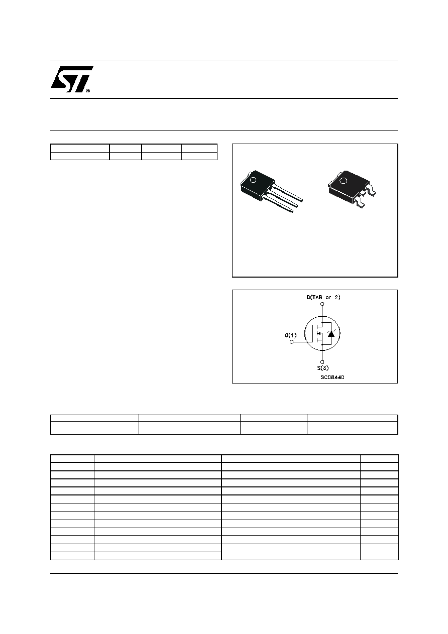
THROUGH-HOLE IPAK (TO-251) POWER
PACKAGE IN TUBE (SUFFIX "-1")
SURFACE-MOUNTING DPAK (TO-252)
POWER PACKAGE IN TAPE & REEL
(SUFFIX "T4")
DESCRIPTION
The STD55NH2LL is based on the latest generation of
ST's proprietary STripFETTM technology. An innovative
layout enables the device to also exhibit extremely low
gate charge for the most demanding requirements as
high-side switch in high-frequency DC-DC converters. It's
therefore ideal for high-density converters in Telecom
and Computer applications.
APPLICATIONS
SPECIFICALLY DESIGNED AND OPTIMISED
FOR HIGH EFFICIENCY DC/DC CONVERTES
TYPE
V
DSS
R
DS(on)
I
D
STD55NH2LL
24 V
< 0.011
40 A(*)
3
2
1
1
3
IPAK
TO-251
(Suffix "-1")
DPAK
TO-252
(Suffix "T4")
Ordering Information
ABSOLUTE MAXIMUM RATINGS
SALES TYPE
MARKING
PACKAGE
PACKAGING
STD55NH2LLT4
STD55NH2LL-1
D55NH2LL
D55NH2LL
TO-252
TO-251
TAPE & REEL
TUBE
Symbol
Parameter
Value
Unit
V
spike(1)
Drain-source Voltage Rating
30
V
V
DS
Drain-source Voltage (V
GS
= 0)
24
V
V
DGR
Drain-gate Voltage (R
GS
= 20 k
)
24
V
V
GS
Gate- source Voltage
± 18
V
I
D
(*)
Drain Current (continuous) at T
C
= 25°C
40
A
I
D
Drain Current (continuous) at T
C
= 100°C
28
A
I
DM(2)
Drain Current (pulsed)
160
A
P
tot
Total Dissipation at T
C
= 25°C
60
W
Derating Factor
0.4
W/°C
E
AS(3)
Single Pulse Avalanche Energy
600
mJ
T
stg
Storage Temperature
-55 to 175
°C
T
j
Operating Junction Temperature
INTERNAL SCHEMATIC DIAGRAM
STD55NH2LL
2/12
THERMAL DATA
ELECTRICAL CHARACTERISTICS (T
CASE
= 25 °C UNLESS OTHERWISE SPECIFIED)
OFF
ON
(4)
DYNAMIC
Rthj-case
Rthj-amb
T
l
Thermal Resistance Junction-case
Thermal Resistance Junction-ambient
Maximum Lead Temperature For Soldering Purpose
Max
Max
2.5
100
275
°C/W
°C/W
°C
Symbol
Parameter
Test Conditions
Min.
Typ.
Max.
Unit
V
(BR)DSS
Drain-source
Breakdown Voltage
I
D
= 250
µ
A, V
GS
= 0
24
V
I
DSS
Zero Gate Voltage
Drain Current (V
GS
= 0)
V
DS
= Max Rating
V
DS
= Max Rating T
C
= 125°C
1
10
µA
µA
I
GSS
Gate-body Leakage
Current (V
DS
= 0)
V
GS
= ± 18V
±100
nA
Symbol
Parameter
Test Conditions
Min.
Typ.
Max.
Unit
V
GS(th)
Gate Threshold Voltage
V
DS
= V
GS
I
D
= 250 µA
1
V
R
DS(on)
Static Drain-source On
Resistance
V
GS
= 10 V
I
D
= 20 A
V
GS
= 4.5 V
I
D
= 20 A
0.010
0.012
0.011
0.0135
Symbol
Parameter
Test Conditions
Min.
Typ.
Max.
Unit
g
fs (4)
Forward Transconductance
V
DS
= 10 V
I
D
= 10 A
18
S
C
iss
C
oss
C
rss
Input Capacitance
Output Capacitance
Reverse Transfer
Capacitance
V
DS
= 10V f = 1 MHz V
GS
= 0
990
385
40
pF
pF
pF
R
G
Gate Input Resistance
f = 1 MHz Gate DC Bias = 0
Test Signal Level = 20 mV
Open Drain
1.3
3/12
STD55NH2LL
SWITCHING ON
SWITCHING OFF
SOURCE DRAIN DIODE
(1)
Garanted when external Rg=4.7
and t
f
< t
fmax
.
(4)
Pulsed: Pulse duration = 300 µs, duty cycle 1.5 %.
(2)
Pulse width limited by safe operating area
(5)
Q
oss =
C
oss
*
V
in ,
C
oss =
C
gd +
C
ds .
See Appendix A
(
3
) Starting T
j
= 25
o
C, I
D
= 20A, V
DD
= 15V
(*)
Value limited by wire bonding
.
Symbol
Parameter
Test Conditions
Min.
Typ.
Max.
Unit
t
d(on)
t
r
Turn-on Delay Time
Rise Time
V
DD
= 10 V
I
D
= 20 A
R
G
= 4.7
V
GS
= 4.5 V
(Resistive Load, Figure 3)
15
56
ns
ns
Q
g
Q
gs
Q
gd
Total Gate Charge
Gate-Source Charge
Gate-Drain Charge
0.44
V
V
DD
10V, I
D
= 40 A
V
GS
= 4.5 V
8.7
4.2
2.4
11
nC
nC
nC
Q
oss(5)
Output Charge
V
DS
= 16 V V
GS
= 0 V
7.6
nC
Symbol
Parameter
Test Conditions
Min.
Typ.
Max.
Unit
t
d(off)
t
f
Turn-off Delay Time
Fall Time
V
DD
= 10 V
I
D
= 20 A
R
G
= 4.7
,
V
GS
= 10 V
(Resistive Load, Figure 3)
13
10
ns
ns
Symbol
Parameter
Test Conditions
Min.
Typ.
Max.
Unit
I
SD
I
SDM
Source-drain Current
Source-drain Current (pulsed)
40
160
A
A
V
SD
(4)
Forward On Voltage
I
SD
= 20 A V
GS
= 0
1.3
V
t
rr
Q
rr
I
RRM
Reverse Recovery Time
Reverse Recovery Charge
Reverse Recovery Current
I
SD
= 40 A
di/dt = 100A/µs
V
DD
= 15 V
T
j
= 150°C
(see test circuit, Figure 5)
32.5
28
1.7
ns
nC
A
ELECTRICAL CHARACTERISTICS (continued)
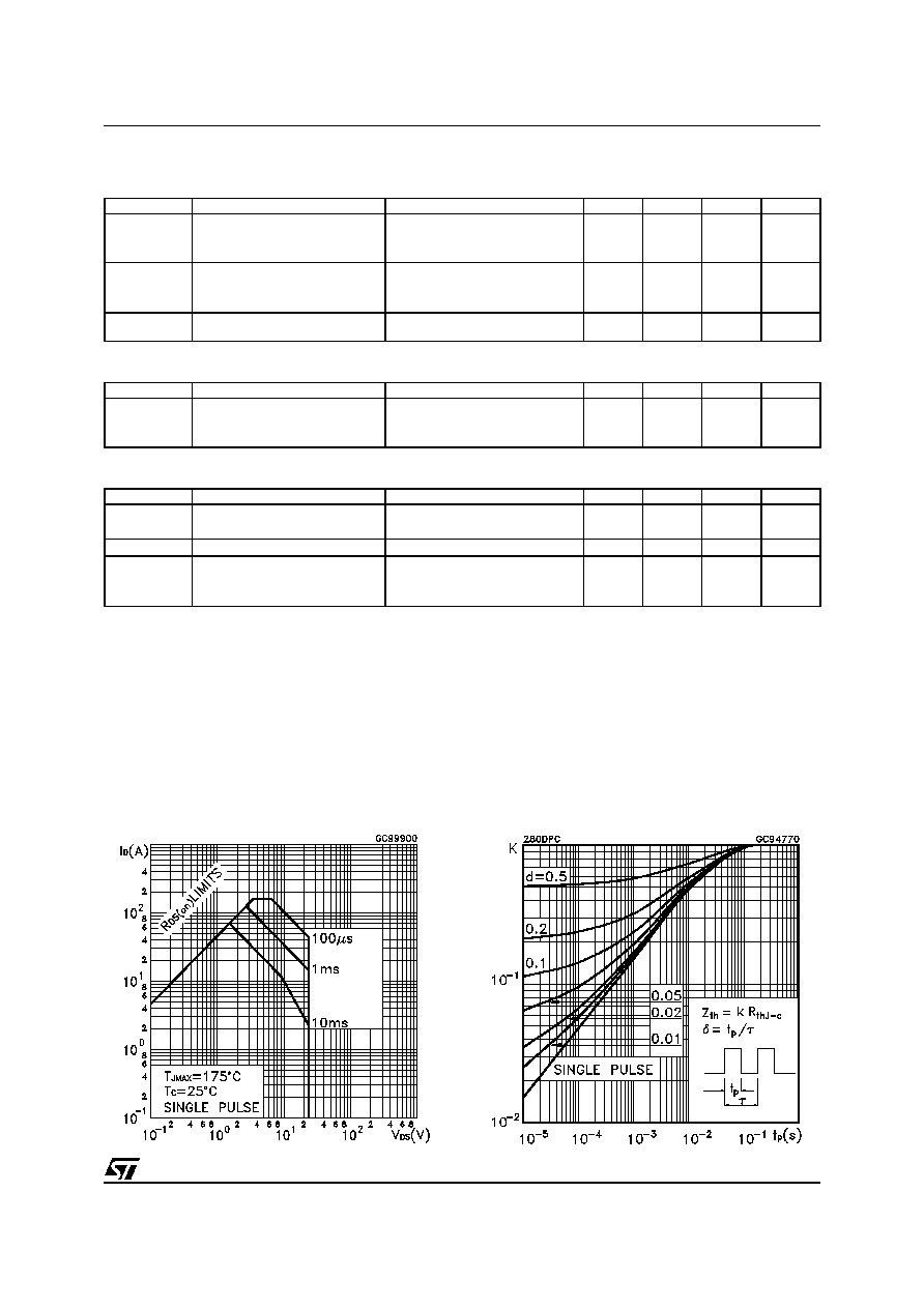
Safe Operating Area
Thermal Impedance
STD55NH2LL
4/12
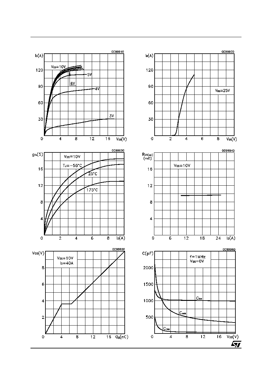
Output Characteristics
Transfer Characteristics
Transconductance
Static Drain-source On Resistance
Gate Charge vs Gate-source Voltage
Capacitance Variations
5/12
STD55NH2LL
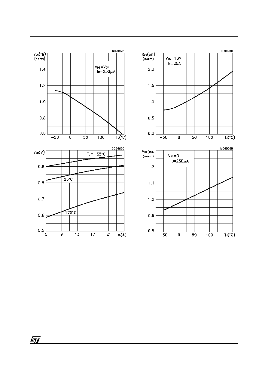
Normalized Gate Threshold Voltage vs Temperature
Normalized on Resistance vs Temperature
Source-drain Diode Forward Characteristics
Normalized Breakdown Voltage vs Temperature
.
.