1/9
October 2002
.
STD20NF10
N-CHANNEL 100V - 0.038
- 25A IPAK/DPAK
LOW GATE CHARGE STripFETTM II POWER MOSFET
s
TYPICAL R
DS
(on) = 0.038
s
EXCEPTIONAL dv/dt CAPABILITY
s
APPLICATION ORIENTED
CHARACTERIZATION
s
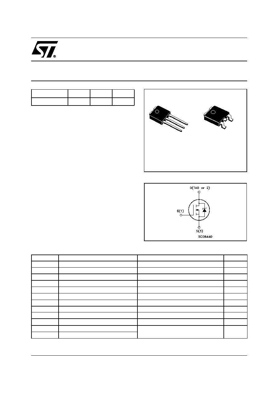
THROUGH-HOLE IPAK (TO-251) POWER
PACKAGE IN TUBE (SUFFIX "-1")
s
SURFACE-MOUNTING DPAK (TO-252)
POWER PACKAGE IN TAPE & REEL
(SUFFIX "T4")
DESCRIPTION
This MOSFET series realized with STMicroelectronics
unique STripFET process has specifically been designed
to minimize input capacitance and gate charge. It is
therefore suitable as primary switch in advanced high-
efficiency, high-frequency isolated DC-DC converters for
Telecom and Computer applications. It is also intended
for any applications with low gate drive requirements.
APPLICATIONS
s
HIGH-EFFICIENCY DC-DC CONVERTERS
s
UPS AND MOTOR CONTROL
TYPE
V
DSS
R
DS(on)
I
D
STD20NF10
100 V
<0.045
25 A(*)
3
2
1
1
3
IPAK
TO-251
(Suffix "-1")
DPAK
TO-252
(Suffix "T4")
ABSOLUTE MAXIMUM RATINGS
(
·)
Pulse width limited by safe operating area.
(*) Current Limited by Package
(1) I
SD
25A, di/dt
300A/µs, V
DD
V
(BR)DSS
, T
j
T
JMAX
(2) Starting T
j
= 25
o
C, I
D
= 10 A, V
DD
= 27V
Symbol
Parameter
Value
Unit
V
DS
Drain-source Voltage (V
GS
= 0)
100
V
V
DGR
Drain-gate Voltage (R
GS
= 20 k
)
100
V
V
GS
Gate- source Voltage
± 20
V
I
D
(*)
Drain Current (continuous) at T
C
= 25°C
25
A
I
D
Drain Current (continuous) at T
C
= 100°C
21
A
I
DM
(
·)
Drain Current (pulsed)
100
A
P
tot
Total Dissipation at T
C
= 25°C
85
W
Derating Factor
0.57
W/°C
dv/dt
(1)
Peak Diode Recovery voltage slope
20
V/ns
E
AS (2)
Single Pulse Avalanche Energy
300
mJ
T
stg
Storage Temperature
-55 to 175
°C
T
j
Operating Junction Temperature
INTERNAL SCHEMATIC DIAGRAM
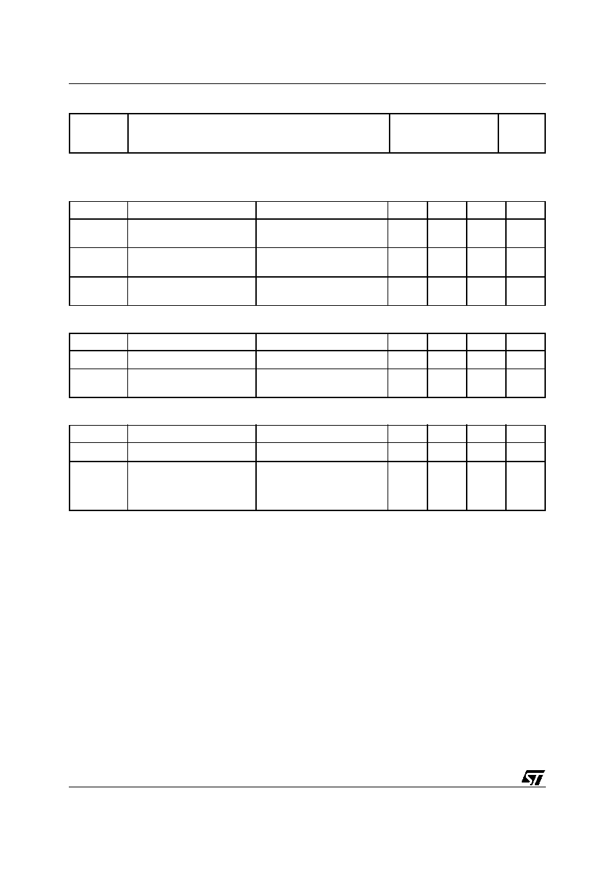
STD20NF10
2/9
THERMAL DATA
ELECTRICAL CHARACTERISTICS (T
CASE
= 25 °C UNLESS OTHERWISE SPECIFIED)
OFF
ON
(1)
DYNAMIC
Rthj-case
Rthj-amb
T
l
Thermal Resistance Junction-case
Thermal Resistance Junction-ambient
Maximum Lead Temperature For Soldering Purpose
Max
Max
Typ
1.76
100
300
°C/W
°C/W
°C
Symbol
Parameter
Test Conditions
Min.
Typ.
Max.
Unit
V
(BR)DSS
Drain-source
Breakdown Voltage
I
D
= 250 µA, V
GS
= 0
100
V
I
DSS
Zero Gate Voltage
Drain Current (V
GS
= 0)
V
DS
= Max Rating
V
DS
= Max Rating T
C
= 125°C
1
10
µA
µA
I
GSS
Gate-body Leakage
Current (V
DS
= 0)
V
GS
= ± 20V
±1
µA
Symbol
Parameter
Test Conditions
Min.
Typ.
Max.
Unit
V
GS(th)
Gate Threshold Voltage
V
DS
= V
GS
I
D
= 250 µA
2
3
4
V
R
DS(on)
Static Drain-source On
Resistance
V
GS
= 10 V
I
D
= 15 A
0.038
0.045
Symbol
Parameter
Test Conditions
Min.
Typ.
Max.
Unit
g
fs (*)
Forward Transconductance
V
DS
= 15 V I
D
= 15 A
10
S
C
iss
C
oss
C
rss
Input Capacitance
Output Capacitance
Reverse Transfer
Capacitance
V
DS
= 25V, f = 1 MHz, V
GS
= 0
1200
180
80
pF
pF
pF
3/9
STD20NF10
SWITCHING ON
SWITCHING OFF
SOURCE DRAIN DIODE
(*)
Pulsed: Pulse duration = 300 µs, duty cycle 1.5 %.
(
·)
Pulse width limited by safe operating area.
Symbol
Parameter
Test Conditions
Min.
Typ.
Max.
Unit
t
d(on)
t
r
Turn-on Delay Time
Rise Time
V
DD
= 50 V
I
D
= 15 A
R
G
= 4.7
V
GS
= 10 V
(Resistive Load, Figure 3)
15
40
ns
ns
Q
g
Q
gs
Q
gd
Total Gate Charge
Gate-Source Charge
Gate-Drain Charge
V
DD
= 80 V I
D
= 30 A V
GS
=10 V
40
8
15
55
nC
nC
nC
Symbol
Parameter
Test Conditions
Min.
Typ.
Max.
Unit
t
d(off)
t
f
Turn-off Delay Time
Fall Time
V
DD
= 50 V
I
D
= 15 A
R
G
= 4.7
,
V
GS
= 10 V
(Resistive Load, Figure 3)
45
10
ns
ns
Symbol
Parameter
Test Conditions
Min.
Typ.
Max.
Unit
I
SD
I
SDM
(
·
)
Source-drain Current
Source-drain Current (pulsed)
30
120
A
A
V
SD
(*)
Forward On Voltage
I
SD
= 20 A V
GS
= 0
1.3
V
t
rr
Q
rr
I
RRM
Reverse Recovery Time
Reverse Recovery Charge
Reverse Recovery Current
I
SD
= 30 A
di/dt = 100A/µs
V
DD
= 55 V
T
j
= 150°C
(see test circuit, Figure 5)
110
390
7.5
ns
µ
C
A
ELECTRICAL CHARACTERISTICS (continued)
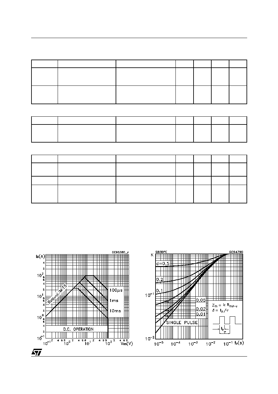
Safe Operating Area
Thermal Impedance
STD20NF10
4/9
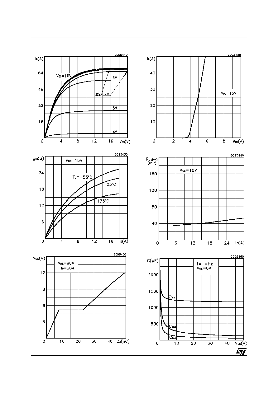
Output Characteristics
Transfer Characteristics
Transconductance
Static Drain-source On Resistance
Gate Charge vs Gate-source Voltage
Capacitance Variations
5/9
STD20NF10
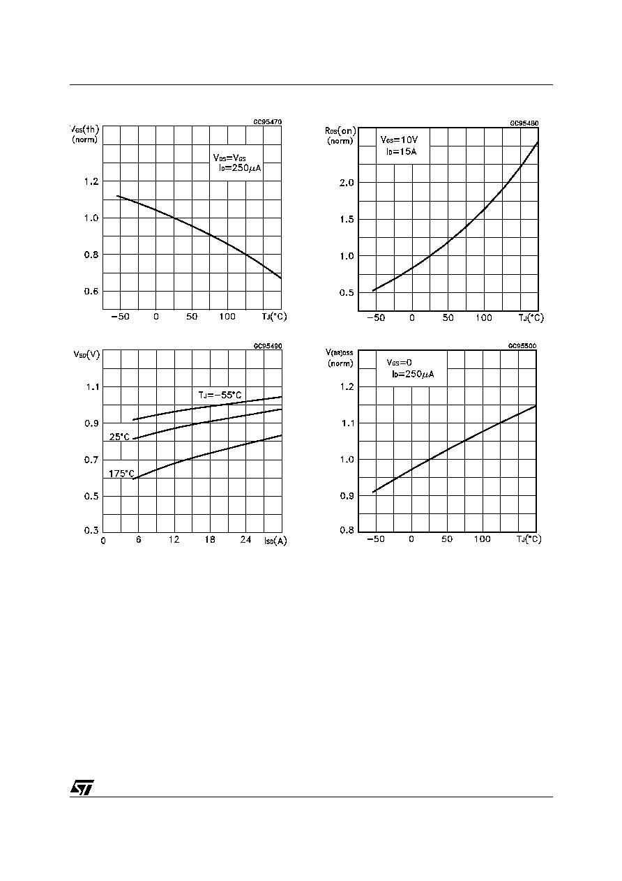
Normalized Gate Threshold Voltage vs Temperature
Normalized
on Resistance vs Temperature
Source-drain Diode Forward Characteristics
Normalized Breakdown Voltage Temperature
.
.