
1/12
PRODUCT PREVIEW
June 2005
This is preliminary information on a new product now in development. Details are subject to change without notice.
STP25NM60N - STF25NM60N
STB25NM60N/-1 - STW25NM60N
N-CHANNEL 600V 0.140
-20A TO-220/FP/D˛/I˛PAK/TO-247
SECOND GENERATION MDmeshTM MOSFET
Table 1: General Features
s
WORLD'S LOWEST ON RESISTANCE
s
TYPICAL R
DS
(on) = 0.140
s
HIGH dv/dt AND AVALANCHE CAPABILITIES
s
100% AVALANCHE TESTED
s
LOW INPUT CAPACITANCE AND GATE
CHARGE
s
LOW GATE INPUT RESISTANCE
DESCRIPTION
The STP25NM60N is realized with the second
generation of MDmesh Technology. This revolu-
tionary MOSFET associates a new vertical struc-
ture to the Company's strip layout to yield the
world's lowest on-resistance and gate charge. It is
therefore suitable for the most demanding high ef-
ficiency converters
APPLICATIONS
The MDmeshTM II family is very suitable for in-
crease the power density of high voltage convert-
ers allowing system miniaturization and higher
efficiencies.
Table 2: Order Code
Figure 1: Package
Figure 2: Internal Schematic Diagram
TYPE
V
DSS
(
@
Tjmax)
R
DS(on)
I
D
STB25NM60N-1
STF25NM60N
STP25NM60N
STW25NM60N
STB25NM60N
650 V
650 V
650 V
650 V
650 V
< 0.170
< 0.170
< 0.170
< 0.170
< 0.170
20 A
20(*) A
20 A
20 A
20 A
TO-247
1
2
3
1
2
3
1
2
3
1
2
3
I
˛
PAK
TO-220
TO-220FP
1
3
D˛PAK
SALES TYPE
MARKING
PACKAGE
PACKAGING
STB25NM60N-1
B25NM60N
I˛PAK
TUBE
STF25NM60N
F25NM60N
TO-220FP
TUBE
STP25NM60N
P25NM60N
TO-220
TUBE
STW25NM60N
W25NM60N
TO-247
TUBE
STB25NM60N
B25NM60N
D˛PAK
TAPE & REEL
Rev. 4
STP25NM60N - STF25NM60N - STB25NM60N/-1 - STW25NM60N
2/12
Table 3: Absolute Maximum ratings
(*) Limited only by maximum temperature allowed
(1) Pulse width limited by safe operating area
(2) I
SD
20 A, di/dt
400 A/µs, V
DD
=80%
V
(BR)DSS
.
Table 4: Thermal Data
Table 5: Avalanche Characteristics
ELECTRICAL CHARACTERISTICS (T
CASE
=25°C UNLESS OTHERWISE SPECIFIED)
Table 6: On /Off
(2) Characteristic value at turn off on inductive load
Symbol
Parameter
Value
Unit
TO-220/I˛PAK
TO-247/D˛PAK
TO-220FP
V
DS
Drain-source Voltage (V
GS
= 0)
600
V
V
DGR
Drain-gate Voltage (R
GS
= 20 k
)
600
V
V
GS
Gate- source Voltage
± 25
V
I
D
Drain Current (continuous) at T
C
= 25°C
20
20 (*)
A
I
D
Drain Current (continuous) at T
C
= 100°C
12.8
12.8 (*)
A
I
DM
(1)
Drain Current (pulsed)
80
80 (*)
A
P
TOT
Total Dissipation at T
C
= 25°C
160
40
W
Derating Factor
1.28
0.32
W/°C
dv/dt (2)
Peak Diode Recovery voltage slope
TBD
V/ns
T
stg
Storage Temperature
55 to 150
°C
T
j
Max. Operating Junction Temperature
150
°C
TO-220/I˛PAK
TO-247/D˛PAK
TO-220FP
Rthj-case
Thermal Resistance Junction-case Max
0.78
3.1
°C/W
Rthj-amb
Thermal Resistance Junction-ambient Max
62.5
°C/W
T
l
Maximum Lead Temperature For Soldering Purpose
300
°C
Symbol
Parameter
Max Value
Unit
I
AS
Avalanche Current, Repetitive or Not-Repetitive
(pulse width limited by T
j
max)
TBD
A
E
AS
Single Pulse Avalanche Energy
(starting T
j
= 25 °C, I
D
= I
AS
, V
DD
= 50 V)
TBD
mJ
Symbol
Parameter
Test Conditions
Value
Unit
Min.
Typ.
Max.
V
(BR)DSS
Drain-source Breakdown
Voltage
I
D
= 1 mA, V
GS
= 0
600
V
dv/dt(2)
Drain Source Voltage
Slope
Vdd=TBD, Id=TBD, Vgs=TBD
TBD
V/ns
I
DSS
Zero Gate Voltage
Drain Current (V
GS
= 0)
V
DS
= Max Rating
V
DS
= Max Rating, T
C
= 125°C
1
10
µA
µA
I
GSS
Gate-body Leakage
Current (V
DS
= 0)
V
GS
= ± 20 V
100
nA
V
GS(th)
Gate Threshold Voltage
V
DS
= V
GS
, I
D
= 250 µA
2
3
4
V
R
DS(on
Static Drain-source On
Resistance
V
GS
= 10 V, I
D
= 10 A
0.140
0.170
3/12
STP25NM60N - STF25NM60N - STB25NM60N/-1 - STW25NM60N
ELECTRICAL CHARACTERISTICS (CONTINUED)
Table 7: Dynamic
Table 8: Source Drain Diode
(1) Pulsed: Pulse duration = 300 µs, duty cycle 1.5 %.
(2) Pulse width limited by safe operating area.
(3) C
oss eq.
is defined as a constant equivalent capacitance giving the same charging time as C
oss
when V
DS
increases from 0 to 80% V
DSS
.
Symbol
Parameter
Test Conditions
Min.
Typ.
Max.
Unit
g
fs
(1)
Forward Transconductance
V
DS
= 15V
,
I
D
= 10A
17
S
C
iss
C
oss
C
rss
Input Capacitance
Output Capacitance
Reverse Transfer
Capacitance
V
DS
= 25 V, f = 1 MHz,
V
GS
= 0
2565
511
77
pF
pF
pF
C
OSS eq
(3)
.
Equivalent Output
Capacitance
V
GS
= 0 V, V
DS
= 0 to 480 V
TBD
pF
R
G
Gate Input Resistance
f=1 MHz Gate DC Bias = 0
Test Signal Level = 20mV
Open Drain
2
t
d(on)
t
r
t
d(off)
t
f
Turn-on Delay Time
Rise Time
Turn-off-Delay Time
Fall Time
V
DD
= 300 V, I
D
= 10 A,
R
G
= 4.7
,
V
GS
= 10 V
(see Figure 4)
TBD
TBD
TBD
TBD
ns
ns
ns
ns
Q
g
Q
gs
Q
gd
Total Gate Charge
Gate-Source Charge
Gate-Drain Charge
V
DD
= 480 V, I
D
= 20 A,
V
GS
= 10 V
(see Figure 7)
93
TBD
TBD
nC
nC
nC
Symbol
Parameter
Test Conditions
Min.
Typ.
Max.
Unit
I
SD
I
SDM
(2)
Source-drain Current
Source-drain Current (pulsed)
20
80
A
A
V
SD
(1)
Forward On Voltage
I
SD
= 20 A, V
GS
= 0
1.3
V
t
rr
Q
rr
I
RRM
Reverse Recovery Time
Reverse Recovery Charge
Reverse Recovery Current
I
SD
= 25 A, di/dt = 100 A/µs
V
DD
= 100V
(see Figure 5)
TBD
TBD
TBD
ns
µC
A
t
rr
Q
rr
I
RRM
Reverse Recovery Time
Reverse Recovery Charge
Reverse Recovery Current
I
SD
= 25 A, di/dt = 100 A/µs
V
DD
= 100V, T
j
= 150°C
(see Figure 5)
TBD
TBD
TBD
ns
µC
A
STP25NM60N - STF25NM60N - STB25NM60N/-1 - STW25NM60N
4/12
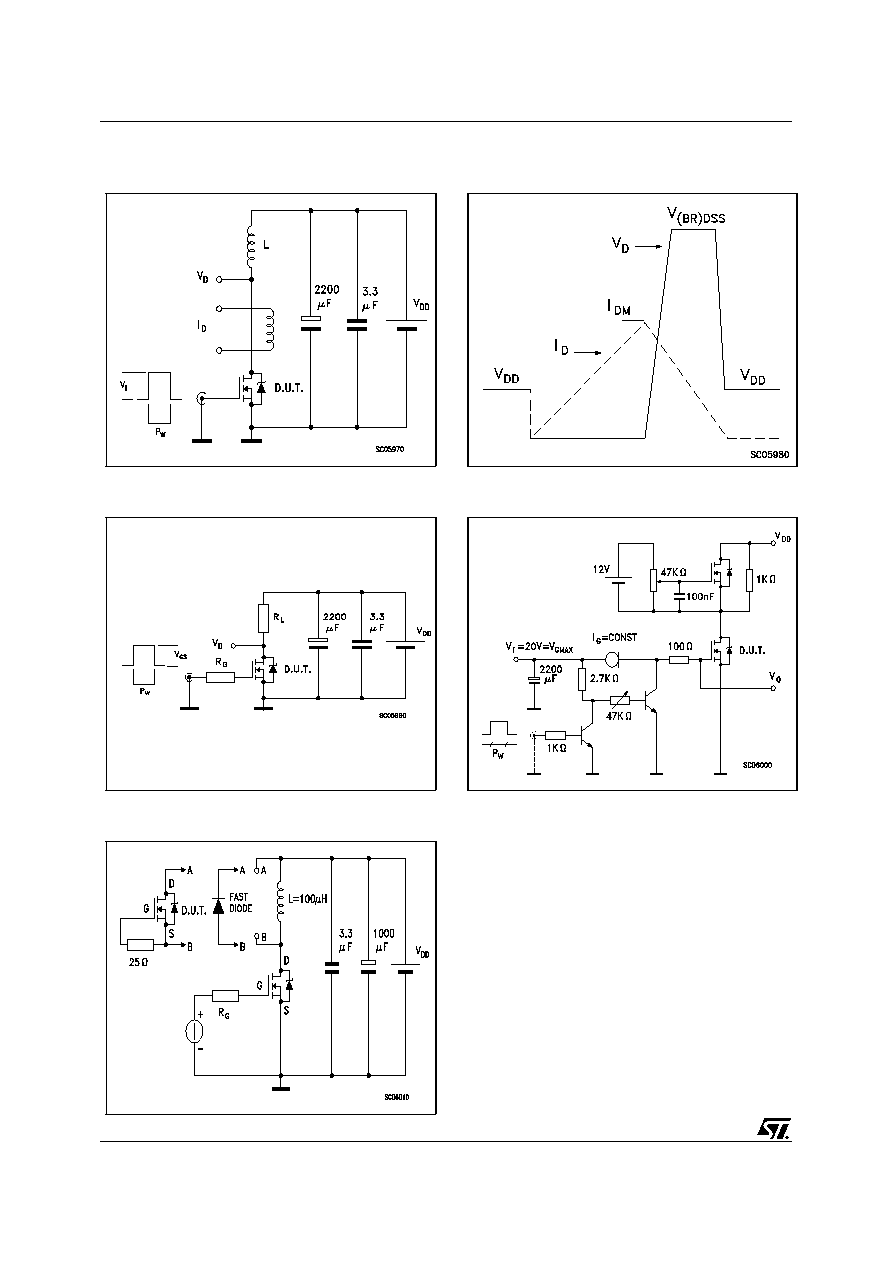
Figure 3: Unclamped Inductive Load Test Cir-
cuit
Figure 4: Switching Times Test Circuit For Re-
sistive Load
Figure 5: Test Circuit For Inductive Load
Switching and Diode Recovery Times
Figure 6: Unclamped Inductive Wafeform
Figure 7: Gate Charge Test Circuit

5/12
STP25NM60N - STF25NM60N - STB25NM60N/-1 - STW25NM60N
DIM.
mm.
inch
MIN.
TYP
MAX.
MIN.
TYP.
MAX.
A
4.40
4.60
0.173
0.181
b
0.61
0.88
0.024
0.034
b1
1.15
1.70
0.045
0.066
c
0.49
0.70
0.019
0.027
D
15.25
15.75
0.60
0.620
E
10
10.40
0.393
0.409
e
2.40
2.70
0.094
0.106
e1
4.95
5.15
0.194
0.202
F
1.23
1.32
0.048
0.052
H1
6.20
6.60
0.244
0.256
J1
2.40
2.72
0.094
0.107
L
13
14
0.511
0.551
L1
3.50
3.93
0.137
0.154
L20
16.40
0.645
L30
28.90
1.137
řP
3.75
3.85
0.147
0.151
Q
2.65
2.95
0.104
0.116
TO-220 MECHANICAL DATA