
ST7536
POWER LINE MODEM
November 1998
.
HALF DUPLEX SYNCHRONOUS FSK MODEM
- TWO PROGRAMMABLE CHANNELS FOR
600BPS DATA RATE
- TWO PROGRAMMABLE CHANNELS FOR
1200BPS DATA RATE
.
AUTOMATICALLYTUNED Rx AND Tx FILTERS
.
TX CARRIER FREQUENCIES SYNTHESIZED
FROM EXTERNAL CRYSTAL
.
LOW DISTORTION Tx SIGNAL (S/H2
50dB)
.
AUTOMATIC LEVELCONTROL ON Tx SIGNAL
.
Rx SENSITIVITY : 2mV
RMS
(600bps)
3mV
RMS
(1200bps)
.
Rx CLOCK RECOVERY
.
POWER-DOWN MODE
.
SUITABLE TO APPLICATION IN ACCORDANCE
WITH DH028/29 ENEL, EN50065-1 CENELEC
AND FCC SPECIFICATIONS
DESCRIPTION
The ST7536 is a half duplex synchronous FSK
MODEM designed for power line communication
network applications.
It operates from a dual power supply +5V and -5V,
and requires an external interface for the coupling
to the power line. It offers two programmable data
rate with two programmable channels each.
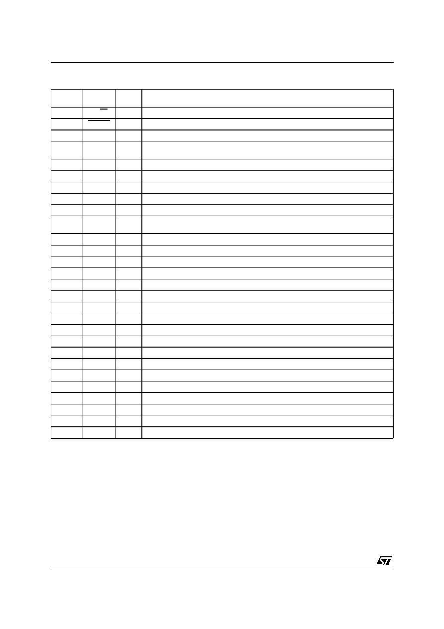
PLCC28
(Plastic Leaded Chip Carrier Package)
ORDER CODE : ST7536CFN
Rx/Tx
18
1
2
3
4
5
6
7
8
9
10
11
19
20
21
22
23
24
25
26
27
28
12
13
14
15
16
17
V
D D
SS
AV
DV
SS
DV
DD
ATO
ALCI
TxFI
RxFO
RAI
AGND
DEMI
IFO
AFCF
BRS
CHS
RESET
TEST
4
TEST
3
TEST 2
TEST 1
CLR/T
RxD
RxDEM
DGND
TxD
XTAL
2
XTAL
1
A
753
6-
01
.
E
P
S
PIN CONNECTIONS
1/9
PIN DESCRIPTION
Pin
Number
Name
Type
Description
1
Rx/Tx
Digital
Rx or Tx mode selection input
2
RESET
Digital
Logic reset and power-down mode input. Active when low.
3
TEST4
Digital
Test input which selects the Tx band-pass filter input (TxFI) when high.
4
TEST3
Digital
Test input which gives an access to the clock recovery input stage. This input is selected
when TEST1 is high.
5
RxD
Digital
Synchronous receive data output
6
CLR/T
Digital
Rx or Tx clock according to the functional mode
7
RxDEM
Digital
Demodulated data output
8
DGND
Supply
Digital ground
9
DV
DD
Supply
Digital positive supply voltage : 5V
±
5%
10
TEST1
Digital
Test input which cancels the Tx to Rx mode automatic switching and validates TEST3
input. Active when high.
11
TEST2
Digital
Test input which reduces the Tx to Rx mode automatic switching time. Active when high.
12
TxD
Digital
Transmit data input
13
XTAL2
Digital
Crystal oscillator output
14
XTAL1
Digital
Crystal oscillator input
15
CHS
Digital
Channel selection input
16
BRS
Digital
Baud rate selection input
17
AFCF
Analog
Automatic frequency control output for connecting compensation network.
18
DV
SS
Supply
Digital negative supply voltage : -5V
±
5%
19
IFO
Analog
Intermediate frequency filter output
20
DEMI
Analog
FSK demodulator input
21
AV
SS
Supply
Analog negative supply voltage : -5V
±
5%
22
AGND
Supply
Analog ground : 0V
23
AV
DD
Supply
Analog positive supply voltage : 5V
±
5%
24
RAI
Analog
Receive analog input
25
RxFO
Analog
Receive filter output
26
TxFI
Analog
Transmit filter input (selected when TEST4 is high)
27
ALCI
Analog
Automatic level control input
28
ATO
Analog
Analog transmit output
7
536-
01
.
T
B
L
ST7536
2/9
FUNCTIONAL DESCRIPTION
1 - Transmit Section
The transmit mode is set when Rx/Tx = 0, if Rx/Tx
is held at 0 longer than 3s, thenthe device switches
automatically in the Rx mode. A new activation of
the Tx mode requires Rx/Tx to be returned to 1 for
a minimum 2
µ
s period before being set to 0.
The Transmit Data (TxD) is sampled on a positive
edge of CLR/T which delivers the transmit bit clock
when the transmit mode is selected. This data
enters a FSK modulator whose two basic frequen-
cies are selected by the Baud Rate Selection pin
(BRS) and the Channel Selection pin (CHS) ac-
cording to the Table 1.
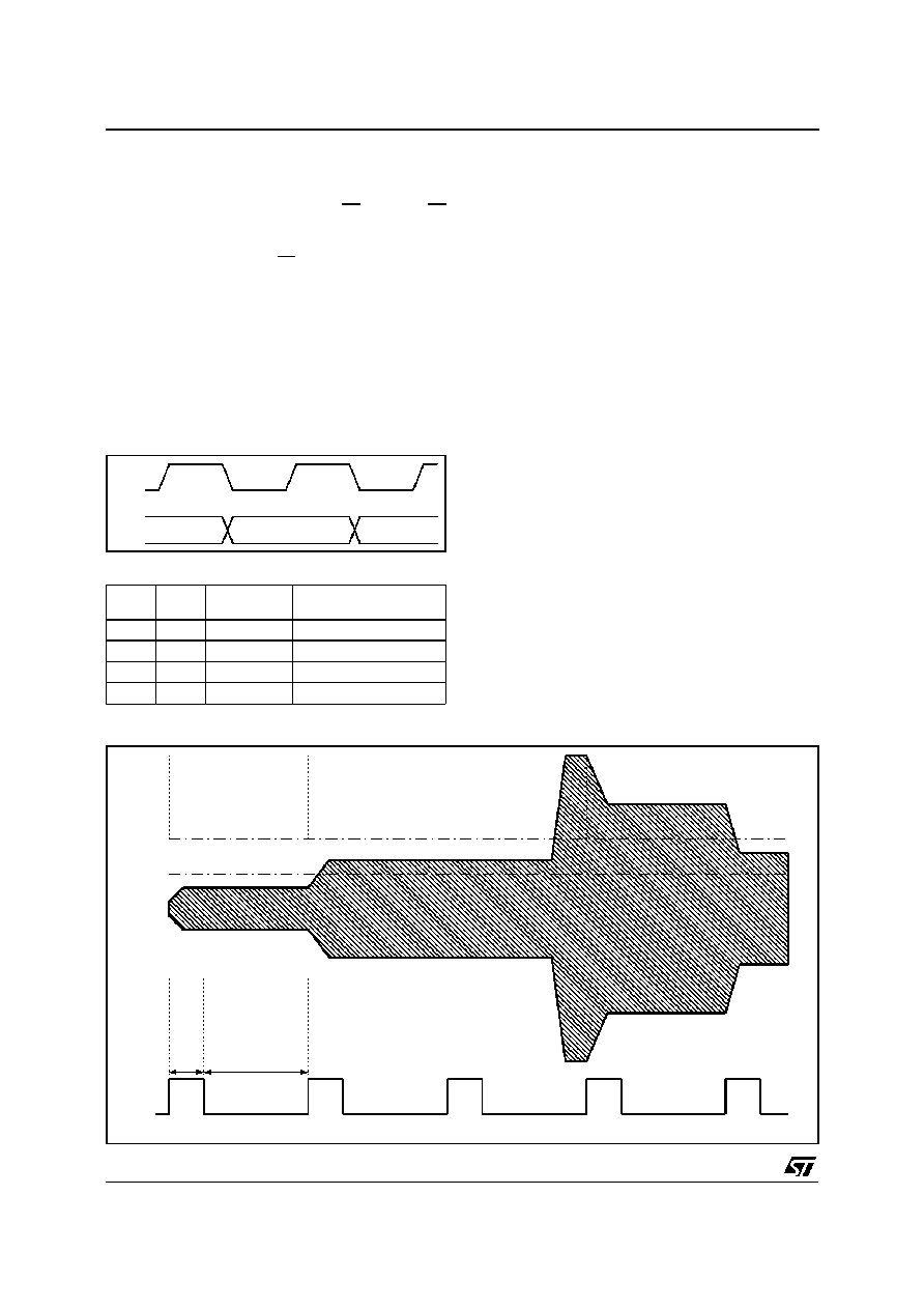
CLR/T
TxD
DATA VALID
75
36-
03.
E
P
S
Figure 1 : Tx Data Input Timing
Table 1
BRS
CHS
Baud Rate
(Baud)
Tx Frequencies (kHz)
TxD=1 - TxD=0
0
0
600
81.75 - 82.35
0
1
600
67.2 - 67.8
1
0
1200
71.4 - 72.6
1
1
1200
85.95 - 87.15
These frequencies are synthesized from a
11.0592MHzcrystal oscillator ; theirprecision is the
same as the crystal one's (100 ppm).
The modulatedsignal coming out of the FSK modu-
lator is filtered by a switched-capacitor band-pass
filter (Tx band-pass) in order to limit the output
spectrum and to reduce the level of harmonic com-
ponents.
The output stage of the Tx path consists of an
Automatic Level Control (ALC) system which keeps
the output signal (ATO) amplitude independant of
the lineimpedancevariations. ThisALC is a variable
gain system (with 32 discrete values) controlled by
an analog feed-back signal ALCI (see Figure 2).
The ALC gain range is 0dB to -26dB and gain
change is clocked at 7200Hz. Gain steps are of
magnitude 0.84dB typically.
A period of this clock is decomposed into a 34.7
µ
s
gain settling latency and a 104.2
µ
s peak detecting
time. The gain change is related to the result of a
peak detection obtained by making a direct com-
parison of ALCI maximum value (during detecting
time) with two threshold voltages V
T1
and V
T2
(see
Figure 2).
- max (VALCI) < V
T1
- The next gain is increased
by 0.84dB,
- V
T1
max (VALCI)
V
T2
- No gain change,
- V
T2
< max (VALCI) - The next gain is decreased
by 0.84dB.
Amplitude
modification
due to an
external cause
High Gain
Low Gain
Correct Gain
Correct
Gain
latency
34.7
µ
s
Gain
setting
Peak
detecting
time
104.2
µ
s
VT2
VT1
ALCI SIGNAL ENVELOP
ALC CLOCK
7536
-
0
4
.
E
P
S
Figure 2 : Automatic Level Control Timing Chart
ST7536
4/9
2 - Receive Section
The receive section is active when Rx/Tx = 1.
The baud rate and channel selection is also made
according to Table 1.
The Rx signal is applied on RAI with a common
mode voltage of 0V and filtered by a band-pass
switched capacitor filter (Rx band-pass) centered
on the received carrier frequency and whose band-
width is around 6kHz. The input voltage range on
RAI is 2mV
RMS
- 2V
RMS
.
The Rx filter output is amplifiedby a 20dBgain stage
whichprovidessymmetrical limitations forlarge volt-
age. The resulting signal is down-converted by a
mixer which receives a local oscillator synthesized
by the FSK modulator block. Finally an intermediate
frequency band-pass filter (IF band-pass) whose
central frequency is 2.7kHz when BRS = 0 and
5.4kHz when BRS = 1 improves the signal to noise
ratio before entering the FSK demodulator. The
coupling of the intermediate frequency filter output
(IFO) to the FSKdemodulatorinput (DEMI) is made
by an externalcapacitor C5 (1
µ
F
±
10%, 10V) which
cancels the Rx path offset voltage.
A clock recovery circuit extracts the receive clock
(CLR/T) from the demodulated output (RxDEM)
and delivers synchronous data (RxD) on the posi-
tive edge of CLR/T.
FUNCTIONAL DESCRIPTION (continued)
3 - Additional Digital and Analog Functions
A reset intput (RESET) initializes the device.
When RESET = 0, the device is in power-down
mode and all the internal logic is reset. When
RESET = 1, the device is active.
A time base section delivers all the internal clocks
from a crystal oscillator (11.0592MHz). The crystal
is connected between XTAL1 and XTAL2 pins and
needs two external capacitors C3 and C4 depend-
ing o n t he cryst al ch ara cte ristic typically
22pF
±
10% for proper operation. It is also possible
to provide directly the clock on pin XTAL1 ; in this
case C3 and C4 should be removed.
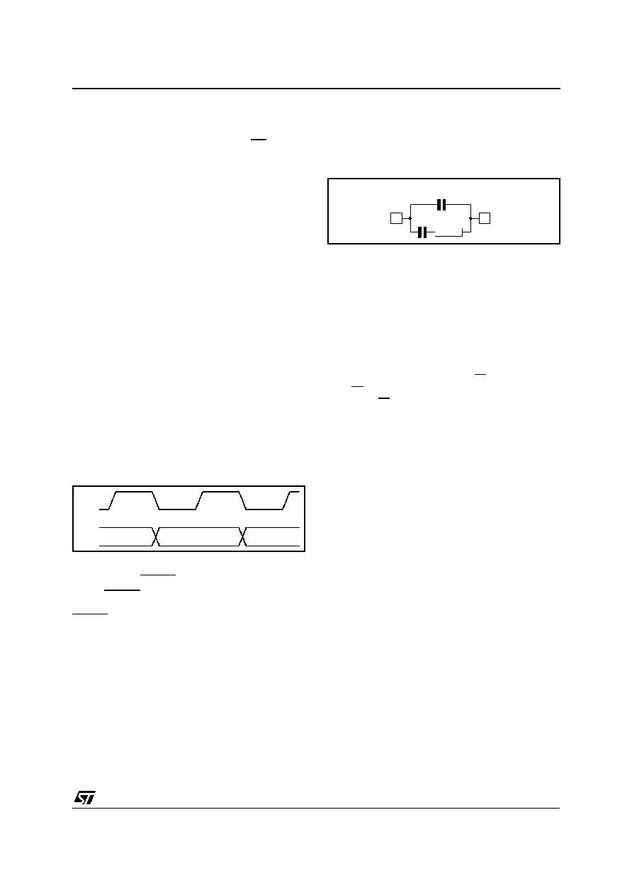
An Automatic Frequency Control (AFC) Section
adjusts the central frequency of Rx and Tx band-
pass filter to the carrier central frequency. The
stability of the AFC loop is ensured by an external
compensation network C1 (470nF
±
10%, 10V), C2
CLR/T
RxD
DATA VALID
753
6-
0
5
.
E
P
S
Figure 3 : Rx Data Output Timing
(47nF
±
10%, 10V) and R1 (1.5k
±
5%) connected
to pin AFCF.
17
C1
C2
R1
AFCF
AGND
22
75
36
-
0
6
.
E
P
S
Figure 4 : Automatic Frequency Loop Filter
4 - Testing Features
- An additionnalamplifier allows the observationof
the Rx band-pass filter output on pin RxFO.
- A direct input to the Tx band-pass filter (TxFI) is
available and selected when TEST4 = 1.
- The 3 second normal duration of the Tx to Rx
mode automatic switching is reduced to 1.48ms
when TEST2 = 1.
- When TEST1 = 1 the Tx to Rx mode automatic
switching is desactivated and the functional mode
of the circuit is controlledby Rx/Tx as follow : when
Rx/Tx = 0 the circuit is transmitting continuously,
whenRx/Tx = 1 the clock recovery block is discon-
nected from the FSK demodulator for testing pur-
pose, in this configuration TEST 3 is the data input
of the clock recovery block, RxDEM follow TEST3
and RxD delivers the resynchronized data.
5 - Power Supplies Wiring and Decoupling
Precautions
The ST7536 has two positive power supply pins,
two negative power supply pins and two ground
pins in order to separate internal analog and digital
supplies. The analog and digital terminals of each
supply pair must be connected together externally
and require special routing precautions in order to
get the best receive sensitivity performances.
The three major routing requirements are :
- The ground impedance should be as low as
possible, for this purpose the AGND an DGND
terminals can be connected via a local plane.
- The positive and negative power supplies (AV
DD
,
DV
DD
, AV
SS
, DV
SS
) should be star-connected,
avoiding common current path for the digital and
analog power supplies terminals.
- Five decoupling capacitors located as close as
possible to the power supply terminals should be
used. Two 2.2
µ
F tantalum and two 100nF ce-
ramic capacitors perform the main decoupling
function in the vicinity of the analog power sup-
plies and a 100nFceramic capacitor in the vicinity
of the positive digital power supply is used to
reduce the high frequency perturbations gener-
ated by the logic part of the circuit.
ST7536
5/9
