Rev. 1.5
April 2003
1/132
ST7263B
LOW SPEED USB 8-BIT MCU FAMILY WITH FLASH/ROM,
UP TO 512 BYTES RAM, 8-BIT ADC, WDG, TIMER, SCI
& I˛C
s
Memories
4, 8 or 16 Kbytes Program Memory: High
Density Flash (HDFlash) or ROM with Read-
out and Write Protection
In-Application Programming (IAP) and In-Cir-
cuit programming (ICP) for HDFlash devices
384 or 512 bytes RAM memory (128-byte
stack)
s
Clock, Reset and Supply Management
Run, Wait, Slow and Halt CPU modes
12 or 24 MHz Oscillator
RAM Retention mode
Optional Low Voltage Detector (LVD)
s
USB (Universal Serial Bus) Interface
DMA for low speed applications compliant
with USB 1.5 Mbs (version 1.1) and HID spec-
ifications (version 1.0)
Integrated 3.3 V voltage regulator and trans-
ceivers
Suspend and Resume operations
3 Endpoints with programmable In/Out config-
uration
s
19 I/O Ports
8 high sink I/Os (10 mA at 1.3 V)
2 very high sink true open drain I/Os (25 mA
at 1.5 V)
8 lines individually programmable as interrupt
inputs
s
2 Timers
Programmable Watchdog
16-bit Timer with 2 Input Captures, 2 Output
Compares, PWM output and clock input
s
2 Communication Interfaces
Asynchronous Serial Communications Inter-
face (on K4 and K2 versions only)
I˛C Multi Master Interface up to 400 kHz
(on K4 versions only)
s
1 Analog Peripheral
8-bit A/D Converter (ADC) with 8 channels
s
Instruction Set
63 basic instructions
17 main addressing modes
8 x 8 unsigned multiply instruction
True bit manipulation
s
Development Tools
Versatile Development Tools (under Win-
dows) including assembler, linker, C-compil-
er, archiver, source level debugger, software
library, hardware emulator, programming
boards and gang programmers
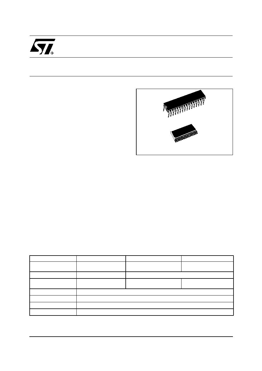
Table 1. Device Summary
SO34 (Shrink)
PSDIP32
Features
ST72F63BK4
ST7263BK2
ST7263BK1
Program Memory -bytes-
16K
(Flash or FASTROM)
8K
(Flash, ROM or FASTROM)
4K
(Flash, ROM or FASTROM)
RAM (stack) - bytes
512 (128)
384 (128)
Peripherals
Watchdog timer, 16-bit tim-
er, SCI, I˛C, ADC, USB
Watchdog timer,
16-bit timer, SCI, ADC, USB
Watchdog, 16-bit timer, ADC,
USB
Operating Supply
4.0 V to 5.5 V
CPU frequency
8 MHz (with 24 MHz oscillator) or 4 MHz (with 12 MHz oscillator)
Operating temperature
0 °C to +70 °C
Packages
SO34/SDIP32
1

Table of Contents
132
2/132
1 INTRODUCTION . . . . . . . . . . . . . . . . . . . . . . . . . . . . . . . . . . . . . . . . . . . . . . . . . . . . . . . . . . . . . . 4
2 PIN DESCRIPTION . . . . . . . . . . . . . . . . . . . . . . . . . . . . . . . . . . . . . . . . . . . . . . . . . . . . . . . . . . . . 5
3 REGISTER & MEMORY MAP . . . . . . . . . . . . . . . . . . . . . . . . . . . . . . . . . . . . . . . . . . . . . . . . . . . . 8
4 FLASH PROGRAM MEMORY . . . . . . . . . . . . . . . . . . . . . . . . . . . . . . . . . . . . . . . . . . . . . . . . . . 11
4.1 INTRODUCTION . . . . . . . . . . . . . . . . . . . . . . . . . . . . . . . . . . . . . . . . . . . . . . . . . . . . . . . . 11
4.2 MAIN FEATURES . . . . . . . . . . . . . . . . . . . . . . . . . . . . . . . . . . . . . . . . . . . . . . . . . . . . . . . 11
4.3 STRUCTURE . . . . . . . . . . . . . . . . . . . . . . . . . . . . . . . . . . . . . . . . . . . . . . . . . . . . . . . . . . . 11
4.4 ICC INTERFACE . . . . . . . . . . . . . . . . . . . . . . . . . . . . . . . . . . . . . . . . . . . . . . . . . . . . . . . . 12
4.5 ICP (IN-CIRCUIT PROGRAMMING) . . . . . . . . . . . . . . . . . . . . . . . . . . . . . . . . . . . . . . . . . 13
4.6 IAP (IN-APPLICATION PROGRAMMING) . . . . . . . . . . . . . . . . . . . . . . . . . . . . . . . . . . . . . 13
5 CENTRAL PROCESSING UNIT . . . . . . . . . . . . . . . . . . . . . . . . . . . . . . . . . . . . . . . . . . . . . . . . . 14
5.1 INTRODUCTION . . . . . . . . . . . . . . . . . . . . . . . . . . . . . . . . . . . . . . . . . . . . . . . . . . . . . . . . 14
5.2 MAIN FEATURES . . . . . . . . . . . . . . . . . . . . . . . . . . . . . . . . . . . . . . . . . . . . . . . . . . . . . . . 14
5.3 CPU REGISTERS . . . . . . . . . . . . . . . . . . . . . . . . . . . . . . . . . . . . . . . . . . . . . . . . . . . . . . . 14
6 RESET AND CLOCK MANAGEMENT . . . . . . . . . . . . . . . . . . . . . . . . . . . . . . . . . . . . . . . . . . . . 17
6.1 RESET . . . . . . . . . . . . . . . . . . . . . . . . . . . . . . . . . . . . . . . . . . . . . . . . . . . . . . . . . . . . . . . . 17
6.2 CLOCK SYSTEM . . . . . . . . . . . . . . . . . . . . . . . . . . . . . . . . . . . . . . . . . . . . . . . . . . . . . . . . 19
7 INTERRUPTS . . . . . . . . . . . . . . . . . . . . . . . . . . . . . . . . . . . . . . . . . . . . . . . . . . . . . . . . . . . . . . . 20
7.1 INTERRUPT REGISTER . . . . . . . . . . . . . . . . . . . . . . . . . . . . . . . . . . . . . . . . . . . . . . . . . . 22
8 POWER SAVING MODES . . . . . . . . . . . . . . . . . . . . . . . . . . . . . . . . . . . . . . . . . . . . . . . . . . . . . 23
8.1 INTRODUCTION . . . . . . . . . . . . . . . . . . . . . . . . . . . . . . . . . . . . . . . . . . . . . . . . . . . . . . . . 23
8.2 HALT MODE . . . . . . . . . . . . . . . . . . . . . . . . . . . . . . . . . . . . . . . . . . . . . . . . . . . . . . . . . . . 23
8.3 SLOW MODE . . . . . . . . . . . . . . . . . . . . . . . . . . . . . . . . . . . . . . . . . . . . . . . . . . . . . . . . . . . 24
8.4 WAIT MODE . . . . . . . . . . . . . . . . . . . . . . . . . . . . . . . . . . . . . . . . . . . . . . . . . . . . . . . . . . . 24
9 I/O PORTS . . . . . . . . . . . . . . . . . . . . . . . . . . . . . . . . . . . . . . . . . . . . . . . . . . . . . . . . . . . . . . . . . . 25
9.1 INTRODUCTION . . . . . . . . . . . . . . . . . . . . . . . . . . . . . . . . . . . . . . . . . . . . . . . . . . . . . . . . 25
9.2 FUNCTIONAL DESCRIPTION . . . . . . . . . . . . . . . . . . . . . . . . . . . . . . . . . . . . . . . . . . . . . . 25
9.3 I/O PORT IMPLEMENTATION . . . . . . . . . . . . . . . . . . . . . . . . . . . . . . . . . . . . . . . . . . . . . . 26
10 MISCELLANEOUS REGISTER . . . . . . . . . . . . . . . . . . . . . . . . . . . . . . . . . . . . . . . . . . . . . . . . 32
11 ON-CHIP PERIPHERALS . . . . . . . . . . . . . . . . . . . . . . . . . . . . . . . . . . . . . . . . . . . . . . . . . . . . . 33
11.1 WATCHDOG TIMER (WDG) . . . . . . . . . . . . . . . . . . . . . . . . . . . . . . . . . . . . . . . . . . . . . . . 33
11.2 16-BIT TIMER . . . . . . . . . . . . . . . . . . . . . . . . . . . . . . . . . . . . . . . . . . . . . . . . . . . . . . . . . . 36
11.3 SERIAL COMMUNICATIONS INTERFACE (SCI) . . . . . . . . . . . . . . . . . . . . . . . . . . . . . . . 55
11.4 USB INTERFACE (USB) . . . . . . . . . . . . . . . . . . . . . . . . . . . . . . . . . . . . . . . . . . . . . . . . . . 67
11.5 I˛C BUS INTERFACE (I˛C) . . . . . . . . . . . . . . . . . . . . . . . . . . . . . . . . . . . . . . . . . . . . . . . . . 75
11.6 8-BIT A/D CONVERTER (ADC) . . . . . . . . . . . . . . . . . . . . . . . . . . . . . . . . . . . . . . . . . . . . . 86
12 INSTRUCTION SET . . . . . . . . . . . . . . . . . . . . . . . . . . . . . . . . . . . . . . . . . . . . . . . . . . . . . . . . . 90
12.1 ST7 ADDRESSING MODES . . . . . . . . . . . . . . . . . . . . . . . . . . . . . . . . . . . . . . . . . . . . . . . 90
12.2 INSTRUCTION GROUPS . . . . . . . . . . . . . . . . . . . . . . . . . . . . . . . . . . . . . . . . . . . . . . . . . 93
13 ELECTRICAL CHARACTERISTICS . . . . . . . . . . . . . . . . . . . . . . . . . . . . . . . . . . . . . . . . . . . . . 96
13.1 PARAMETER CONDITIONS . . . . . . . . . . . . . . . . . . . . . . . . . . . . . . . . . . . . . . . . . . . . . . . 96
13.2 ABSOLUTE MAXIMUM RATINGS . . . . . . . . . . . . . . . . . . . . . . . . . . . . . . . . . . . . . . . . . . . 97

Table of Contents
3/132
13.3 OPERATING CONDITIONS . . . . . . . . . . . . . . . . . . . . . . . . . . . . . . . . . . . . . . . . . . . . . . . . 98
13.4 SUPPLY CURRENT CHARACTERISTICS . . . . . . . . . . . . . . . . . . . . . . . . . . . . . . . . . . . 100
13.5 CLOCK AND TIMING CHARACTERISTICS . . . . . . . . . . . . . . . . . . . . . . . . . . . . . . . . . . 101
13.6 MEMORY CHARACTERISTICS . . . . . . . . . . . . . . . . . . . . . . . . . . . . . . . . . . . . . . . . . . . 103
13.7 EMC CHARACTERISTICS . . . . . . . . . . . . . . . . . . . . . . . . . . . . . . . . . . . . . . . . . . . . . . . 104
13.8 I/O PORT PIN CHARACTERISTICS . . . . . . . . . . . . . . . . . . . . . . . . . . . . . . . . . . . . . . . . 109
13.9 CONTROL PIN CHARACTERISTICS . . . . . . . . . . . . . . . . . . . . . . . . . . . . . . . . . . . . . . . 114
13.10COMMUNICATION INTERFACE CHARACTERISTICS . . . . . . . . . . . . . . . . . . . . . . . . 116
13.118-BIT ADC CHARACTERISTICS . . . . . . . . . . . . . . . . . . . . . . . . . . . . . . . . . . . . . . . . . . 119
14 PACKAGE CHARACTERISTICS . . . . . . . . . . . . . . . . . . . . . . . . . . . . . . . . . . . . . . . . . . . . . . 121
14.1 PACKAGE MECHANICAL DATA . . . . . . . . . . . . . . . . . . . . . . . . . . . . . . . . . . . . . . . . . . . 121
14.2 THERMAL CHARACTERISTICS . . . . . . . . . . . . . . . . . . . . . . . . . . . . . . . . . . . . . . . . . . 122
14.3 SOLDERING AND GLUEABILITY INFORMATION . . . . . . . . . . . . . . . . . . . . . . . . . . . . . 123
15 DEVICE CONFIGURATION AND ORDERING INFORMATION . . . . . . . . . . . . . . . . . . . . . . . 124
15.1 OPTION BYTE . . . . . . . . . . . . . . . . . . . . . . . . . . . . . . . . . . . . . . . . . . . . . . . . . . . . . . . . . 124
15.2 DEVICE ORDERING INFORMATION . . . . . . . . . . . . . . . . . . . . . . . . . . . . . . . . . . . . . . . 125
15.3 DEVELOPMENT TOOLS . . . . . . . . . . . . . . . . . . . . . . . . . . . . . . . . . . . . . . . . . . . . . . . . . 126
15.4 ST7 APPLICATION NOTES . . . . . . . . . . . . . . . . . . . . . . . . . . . . . . . . . . . . . . . . . . . . . . 128
16 KNOWN LIMITATIONS . . . . . . . . . . . . . . . . . . . . . . . . . . . . . . . . . . . . . . . . . . . . . . . . . . . . . . 130
16.1 UNEXPECTED RESET FETCH . . . . . . . . . . . . . . . . . . . . . . . . . . . . . . . . . . . . . . . . . . . . 130
16.2 HALT MODE POWER CONSUMPTION WITH ADC ON . . . . . . . . . . . . . . . . . . . . . . . . . 130
17 SUMMARY OF CHANGES . . . . . . . . . . . . . . . . . . . . . . . . . . . . . . . . . . . . . . . . . . . . . . . . . . . 131
To obtain the most recent version of this datasheet,
please check at www.st.com>products>technical literature>datasheet
Please also pay special attention to the Section "IMPORTANT NOTES" on page 130.
ST7263B
4/132
1 INTRODUCTION
The ST7263B Microcontrollers form a sub-family
of the ST7 MCUs dedicated to USB applications.
The devices are based on an industry-standard 8-
bit core and feature an enhanced instruction set.
They operate at a 24 MHz or 12 MHz oscillator fre-
quency. Under software control, the ST7263B
MCUs may be placed in either Wait or Halt modes,
thus reducing power consumption. The enhanced
instruction set and addressing modes afford real
programming potential. In addition to standard 8-
bit data management, the ST7263B MCUs feature
true bit manipulation, 8x8 unsigned multiplication
and indirect addressing modes. The devices in-
clude an ST7 Core, up to 16 Kbytes of program
memory, up to 512 bytes of RAM, 19 I/O lines and
the following on-chip peripherals:
USB low speed interface with 3 endpoints with
programmable in/out configuration using the
DMA architecture with embedded 3.3V voltage
regulator and transceivers (no external compo-
nents are needed).
8-bit Analog-to-Digital converter (ADC) with 8
multiplexed analog inputs
Industry standard asynchronous SCI serial inter-
face (not on all products - see
Table 1
Device
Summary)
Watchdog
16-bit Timer featuring an External clock input, 2
Input Captures, 2 Output Compares with Pulse
Generator capabilities
Fast I˛C Multi Master interface (not on all prod-
ucts - see device summary)
Low voltage reset (LVD) ensuring proper power-
on or power-off of the device
The ST7263B devices are ROM versions.
The ST72P63B devices are Factory Advanced
Service Technique ROM (FASTROM) versions:
they are factory-programmed and are not repro-
grammable.
The ST72F63B devices are Flash versions. They
support programming in IAP mode (In-application
programming) via the on-chip USB interface.
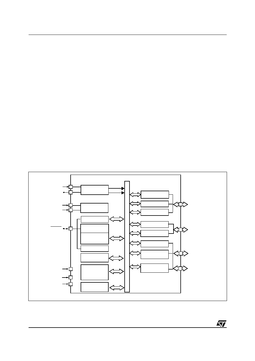
Figure 1. General Block Diagram
8-BIT CORE
ALU
A
DDRE
S
S
A
ND DA
T
A
B
U
S
OSCIN
OSCOUT
RESET
PORT B
16-BIT TIMER
PORT A
PORT C
PB[7:0]
(8 bits)
PC[2:0]
(3 bits)
OSCILLATOR
INTERNAL
CLOCK
CONTROL
RAM
(384/512 Bytes)
PA[7:0]
(8 bits)
V
SS
V
DD
POWER
SUPPLY
SCI*
PROGRAM
(4K/8K/16K Bytes)
I˛C*
MEMORY
ADC
(UART)
USB SIE
OSC/3
LVD
WATCHDOG
V
SSA
V
DDA
V
PP
/TEST
USB DMA
USBDP
USBDM
USBVCC
OSC/4 or OSC/2
(for USB)
* Not on all products (refer to Table 1: Device Summary)
ST7263B
5/132
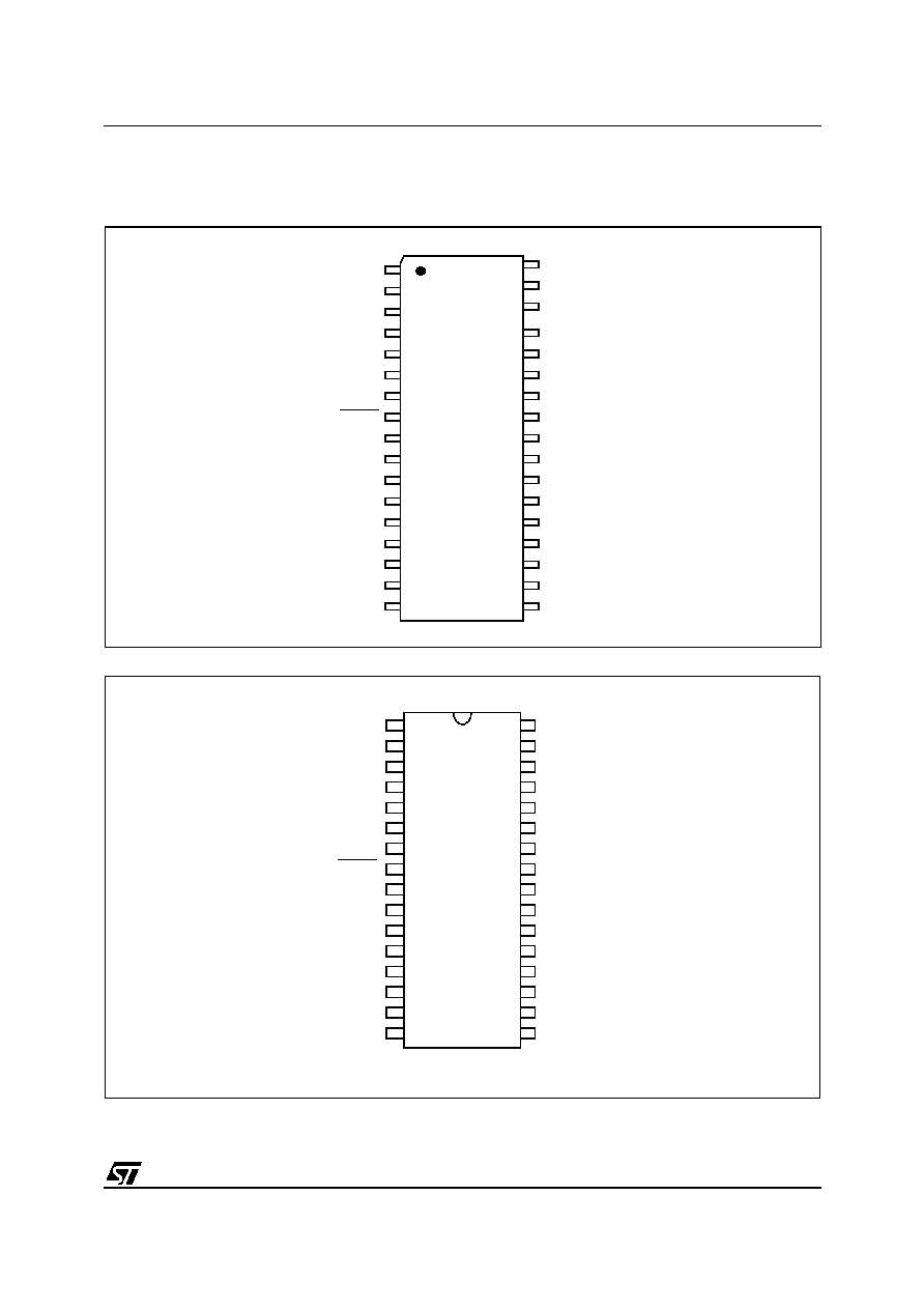
2 PIN DESCRIPTION
Figure 2. 34-Pin SO Package Pinout
Figure 3. 32-Pin SDIP Package Pinout
18
19
20
21
22
23
31
30
29
28
27
26
25
24
1
2
3
4
5
6
7
8
9
10
11
12
13
14
V
DD
OSCOUT
AIN4/IT5/PB4
(10mA)
AIN5/IT6/PB5
(10mA)
V
PP
/TEST
AIN6/PB6/IT7
(10mA)
AIN7/IT8PB7
(10mA)
NC
RESET
PC0/RDI
PC1/TDO
PC2/USBOE
V
SS
OSCIN
USBDP
V
SSA
PB0
(10mA)/AIN0
PA7/OCMP2/IT4
PA6/OCMP1/IT3
PA5/ICAP2/IT2
PA4/ICAP1/IT1
PA3/EXTCLK
PA2
(25mA)/SCL/ICCCLK
NC
NC
NC
PA1
(25mA)/SDA/ICCDATA
PA0/MCO
15
16
17
AIN1/PB1
(10mA)
AIN2/PB2
(10mA)
AIN3/PB3
(10mA)
34
33
32
V
DDA
USBVCC
USBDM
* V
PP
on Flash versions only
28
27
26
25
24
23
22
21
20
19
18
17
16
15
1
2
3
4
5
6
7
8
9
10
11
12
13
14
29
30
31
32
V
DD
OSCOUT
AIN1/PB1/
(10mA)
AIN2/PB2
(10mA)
AIN3/PB3
(10mA)
AIN4/IT5/PB4
(10mA)
AIN5/IT6/PB5
(10mA)
V
PP
/TEST*
AIN6/IT7/PB6
(10mA)
PC0/RDI
PC1/TDO
PC2/USBOE
V
SS
OSCIN
AIN7/IT8/PB7
(10mA)
RESET
V
DDA
USBVCC
PB0
(10mA)/AIN0
PA7/COMP2/IT4
PA6/COMP1/IT3
PA5/ICAP2/IT2
PA4/ICAP1/IT1
PA3/EXTCLK
PA2
(25mA)/SCL/ICCCLK
PA1
(25mA)/SDA/ICCDATA
PA0/MCO
V
SSA
USBDP
USBDM
NC
NC
* V
PP
on Flash versions only