1/12
July 2003
s
LOW SUPPLY CURRENT: 5mA MAX
s
DESIGNED FOR RS485 INTERFACE
APPLICATIONS
s
-7 TO 12 COMMON MODE INPUT VOLTAGE
RANGE
s
70mV TYPICAL INPUT HYSTERESIS
s
DESIGNED FOR 25Mbps OPERATION
s
OPERATE FROM SINGLE 5 SUPPLY
s
±4kV ESD PROTECTION
s
CURRENT LIMITING AND THERMAL
SHUTDOWN FOR DRIVER OVERLOAD
PROTECTION
DESCRIPTION
The ST491A is a low power transceiver for
RS-485 and RS-422 communications. The device
contains one driver and one receiver in full duplex
configuration. The ST491A draws 5mA (typ.) of
supply current when unloaded and operates from
a single 5V supply.
Driver is short-circuit current limited and is
protected against excessive power dissipation by
thermal shutdown circuitry that place the driver
outputs into a high-impedance state. The receiver
input has a fail-safe feature that guarantees a
logic high output if both inputs are open circuit.
ORDERING CODES
Type
Temperature
Range
Package
Comments
ST491ACN
0 to 70 °C
DIP-14
25parts per tube / 40tube per box
ST491ABN
-40 to 85 °C
DIP-14
25parts per tube / 40tube per box
ST491ACD
0 to 70 °C
SO-14 (Tube)
50parts per tube / 20tube per box
ST491ABD
-40 to 85 °C
SO-14 (Tube)
50parts per tube / 20tube per box
ST491ACDR
0 to 70 °C
SO-14 (Tape & Reel)
2500 parts per reel
ST491ABDR
-40 to 85 °C
SO-14 (Tape & Reel)
2500 parts per reel
ST491A
LOW POWER HIGH SPEED RS-485/RS-422 TRANSCEIVER
DIP
SOP
ST491A
2/12
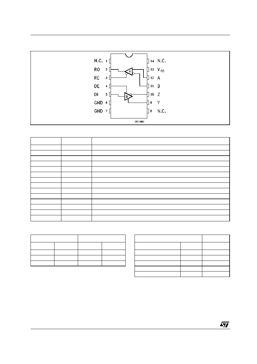
PIN CONFIGURATION
PIN DESCRIPTION
TRUTH TABLE (DRIVER)
X= Don't Care; Z=High Impedance
TRUTH TABLE (RECEIVER)
?= Irrelevant; X= Don't Care; Z=High Impedance
PlN N°
SYMBOL
NAME AND FUNCTION
1
NC
Not Connected
2
RO
Receiver Output.
3
RE
Receiver Output Enable
4
DE
Driver Output Enable
5
DI
Inverting Driver Input.
6
GND
Ground
7
GND
Ground
8
NC
Not Connected
9
Y
Non-inverting Driver Output
10
Z
Inverting Driver Output
11
B
Inverting Receiver Input
12
A
Non-inverting Receiver Input
13
NC
Not Connected
14
V
CC
Supply Voltage
INPUT
OUTPUTS
DI
DE
Y
Z
L
H
L
H
H
H
H
L
X
L
Z
Z
INPUT
OUTPUT
A-B
RE
RO
-0.2V
L
H
between -0.2V to 0.2V
L
?
-0.2V
L
L
OPEN
L
H
X
H
Z
ST491A
3/12
ABSOLUTE MAXIMUM RATINGS
Absolute Maximum Ratings are those values beyond which damage to the device may occur. Functional operation under these condition is
not implied.
ELECTRICAL CHARACTERISTICS
V
CC
= 4.5V to 5.5V, T
A
= -40 to 85°C, unless otherwise specified. Typical values are referred to T
A
= 25°C)
TRANSMITTER ELECTRICAL CHARACTERISTICS
V
CC
= 4.5V to 5.5V, T
A
= -40 to 85°C, unless otherwise specified. Typical values are referred to T
a
= 25°C)
Symbol
Parameter
Value
Unit
V
CC
Supply Voltage
7
V
V
DI
Driver Input Voltage
-0.5 to 7
V
V
Y
, V
Z
Driver Output Voltage
-7.5 to 12.5
V
V
A
, V
B
Receiver Input Voltage
-7.5 to 12.5
V
V
RO
Receiver Output Voltage
-0.3 to (V
CC
+ 0.3)
V
ESD
Human Body Model
3.5
KV
Symbol
Parameter
Test Conditions
Min.
Typ.
Max.
Unit
I
SUPPLY
No Load Supply Current
2
5
mA
C
IN
Input Capacitance
1.8
pF
C
YZ
Driver Output Capacitance
1.2
pF
C
OUT
Output Capacitance
2.3
pF
Symbol
Parameter
Test Conditions
Min.
Typ.
Max.
Unit
V
OD1
Differential Drive Output
(No load)
V
CC
V
V
OD2
Differential Drive Output
(With Load)
R
L
= 54
(RS-422) (Figure 1)
1.5
2.6
5
V
V
OD3
Differential Drive Output
(With Load)
R
L
= 100
(RS-422) (Figure 1)
2
3
V
V
OD
Change in magnitude of
Driver Differential Output
Voltage for Complementary
Output States (Note1)
R
L
= 54
or 100
(Figure 1)
0
0.2
V
V
OC
Driver Common Mode
Output Voltage
R
L
= 54
(Figure 1)
1
3
V
V
OC
Change in magnitude of
Driver Common Mode
Output Voltage (Note1)
R
L
= 54
(Figure 1)
0
0.2
V
I
OFF
Power Off Output Current
V
CC
= 0V
V
O
=-7V to 12V
±
100
µ
A
I
OSD
Driver Short Circuit Output
Current
V
O
=-7V to 12V
±
35
±
250
mA
V
IL
Input Logic Threshold Low
0.8
V
V
IH
Input Logic Threshold High
2
V

ST491A
4/12
RECEIVER ELECTRICAL CHARACTERISTICS
V
CC
= 4.5V to 5.5V, T
A
= -40 to 85°C, unless otherwise specified. Typical values are referred to T
a
= 25°C)
DRIVER SWITCHING CHARACTERISTICS
V
CC
= 4.5V to 5.5V, T
A
= -40 to 85°C, unless otherwise specified. Typical values are referred to T
a
= 25°C)
RECEIVER SWITCHING CHARACTERISTICS
V
CC
= 4.5V to 5.5V, T
A
= -40 to 85°C, unless otherwise specified. Typical values are referred to T
a
= 25°C)
Symbol
Parameter
Test Conditions
Min.
Typ.
Max.
Unit
I
IN
Input Current (A, B)
other input=0V
V
CC
= 0 or 5.25V
V
IN
=12V
0.5
1
mA
V
IN
=-7V
-0.35
-0.8
mA
V
TH
Receiver Differential
Threshold Voltage
V
CM
= -7V to 12V
-0.2
0.2
V
V
TH
Receiver Input Hysteresis
V
CM
= 0V
70
mV
V
OH
Receiver Output High
Voltage
I
OUT
= -8mA, V
ID
= 200mV
3.5
4.7
V
V
OL
Receiver Output Low
Voltage
I
OUT
= 8mA, V
ID
= -200mV
0.3
0.5
V
R
RIN
Receiver Input Resistance
V
CM
= -7V to 12V
12
24
K
Symbol
Parameter
Test Conditions
Min.
Typ.
Max.
Unit
D
R
Maximum Data Rate
Jitter <5%
25
50
Mbps
t
PLH
t
PHL
Propagation Delay Input to
Output
R
L
= 54
C
L1
=C
L2
=50pF, (Figure 1)
10
16
ns
t
SKEW
Differential Output Delay
Skew
R
L
= 54
C
L1
=C
L2
=50pF, (Figure 1)
1
3
ns
t
TLH
t
THL
Rise or Fall Differential
Time
R
L
= 54
C
L1
=C
L2
=50pF, (Figure 1)
8
12
ns
t
PZL
Output Enable Time
C
L
= 50pF
S1 Closed
14
25
ns
t
PZH
Output Enable Time
C
L
= 50pF
S2 Closed
14
25
ns
t
PHZ
Output Disable Time
C
L
= 15pF
S2 Closed
10
25
ns
t
PLZ
Output Disable Time
C
L
= 15pF
S1 Closed
16
25
ns
Symbol
Parameter
Test Conditions
Min.
Typ.
Max.
Unit
t
PLH
t
PHL
Propagation Delay Input to
Output
C
L
= 15pF
(Figures 2,4)
19
30
ns
t
SKD
|t
PLH -
t
PHL
| Receiver Output
Skew
C
L
= 15pF
(Figures 2,4)
1
3
ns
t
TLH
t
THL
Rise or Fall Time
C
L
= 15pF
(Figures 2,4)
6
ns
t
PZL
Output Enable Time
C
RL
= 15pF
S1 Closed
6
12
ns
t
PZH
Output Enable Time
C
RL
= 15pF
S2 Closed
7
12
ns
t
PHZ
Output Disable Time
C
RL
= 15pF
S2 Closed
6
12
ns
t
PLZ
Output Disable Time
C
RL
= 15pF
S1 Closed
6
12
ns
ST491A
5/12
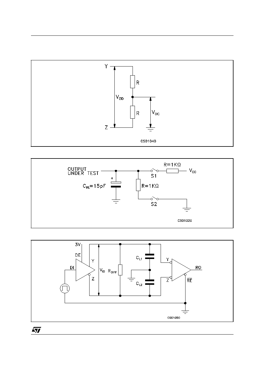
TEST CIRCUITS AND TYPICAL CHARACTERISTICS
Figure 1 : Driver DC Test Load
Figure 2 : Receiver Timing Test Load
Figure 3 : Driver/Receiver Timing Test Circuit