USE IN LIFE SUPPORT DEVICES OR SYSTEMS MUST BE EXPRESSLY AUTHORIZED.
ST PRODUCTS ARE NOT AUTHORIZED FOR USE AS CRITICAL COMPONENTS IN LIFE SUPPORT DEVICES OR
SYSTEMS WITHOUT THE EXPRESS WRITTEN APPROVAL OF STMicroelectronics.
As used herein:
1. Life support devices or systems are those which (a)
are intended for surgical implant into the body, or (b)
support or sustain life, and whose failure to perform,
when properly used in accordance with instructions for
use provided with the product, can be reasonably ex-
pected to result in significant injury to the user.
2. A critical component is any component of a life sup-
port device or system whose failure to perform can rea-
sonably be expected to cause the failure of the life
support device or system, or to affect its safety or effec-
tiveness.
The present document contains CONFIDENTIAL INFORMATION.
Please refer to last page for obligations
i/iv
FSD_CHIPSET_B/0104VP2
CHIP SET INTERFACE SPECIFICATION
i
DIFFERENCES BETWEEN:
FSD_CHIPSET_B/0006VP1
AND
FSD_CHIPSET_B/0104VP2
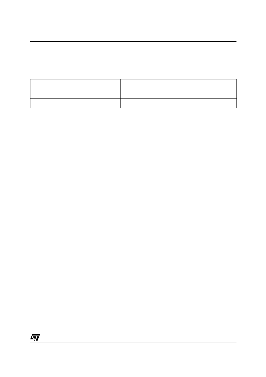
Note: other modifications which are only editorial are not described in this table.
DESCRIPTION OF THE MODIFICATION
PARAGRAPH ON VP2
Definition modification of the signal Tx-start
Chapter 1.2.2 "Interface signals definition", page 2
Modification of the figure 4
Chapter 1.7 "FPGA pin-out & Chip Set Block Diagram", page 8

ii/iv
CHIP SET INTERFACE SPECIFICATION
FSD_CHIPSET_B/0104VP2
TABLE OF CONTENTS
1 FPGA & MCU INTERFACE . . . . . . . . . . . . . . . . . . . . . . . . . . . . . . . . . . . . . . . . . . . . . . . . . . . . . 1
1.1 DESCRIPTION . . . . . . . . . . . . . . . . . . . . . . . . . . . . . . . . . . . . . . . . . . . . . . . . . . . . . . . . . . . 1
1.2 PHYSICAL INTERFACE BETWEEN FPGA AND MCU . . . . . . . . . . . . . . . . . . . . . . . . . . . . 1
1.2.1 Interface signals description . . . . . . . . . . . . . . . . . . . . . . . . . . . . . . . . . . . . . . . . . . . 1
1.2.2 Interface signals definition . . . . . . . . . . . . . . . . . . . . . . . . . . . . . . . . . . . . . . . . . . . . . 2
1.3 FIFOS ACCESS . . . . . . . . . . . . . . . . . . . . . . . . . . . . . . . . . . . . . . . . . . . . . . . . . . . . . . . . . . 2
1.3.1 Transmission FIFO (cf figure 1) . . . . . . . . . . . . . . . . . . . . . . . . . . . . . . . . . . . . . . . . . 2
1.3.2 Reception FIFO (cf figures 2 & 3) . . . . . . . . . . . . . . . . . . . . . . . . . . . . . . . . . . . . . . . 2
1.3.3 Write access chronogram . . . . . . . . . . . . . . . . . . . . . . . . . . . . . . . . . . . . . . . . . . . . . 3
1.3.4 Read access chronogram . . . . . . . . . . . . . . . . . . . . . . . . . . . . . . . . . . . . . . . . . . . . . 3
1.3.5 MCU interface timings . . . . . . . . . . . . . . . . . . . . . . . . . . . . . . . . . . . . . . . . . . . . . . . . 4
1.4 CONTROL REGISTERS . . . . . . . . . . . . . . . . . . . . . . . . . . . . . . . . . . . . . . . . . . . . . . . . . . . 5
1.4.1 Reception control bits . . . . . . . . . . . . . . . . . . . . . . . . . . . . . . . . . . . . . . . . . . . . . . . . 5
1.4.2 Transmission Control bits . . . . . . . . . . . . . . . . . . . . . . . . . . . . . . . . . . . . . . . . . . . . . 5
1.4.3 Others Control bits . . . . . . . . . . . . . . . . . . . . . . . . . . . . . . . . . . . . . . . . . . . . . . . . . . . 5
1.5 STATUS REGISTER . . . . . . . . . . . . . . . . . . . . . . . . . . . . . . . . . . . . . . . . . . . . . . . . . . . . . . 6
1.6 REGISTERS MAPPING . . . . . . . . . . . . . . . . . . . . . . . . . . . . . . . . . . . . . . . . . . . . . . . . . . . . 7
1.6.1 Control Registers . . . . . . . . . . . . . . . . . . . . . . . . . . . . . . . . . . . . . . . . . . . . . . . . . . . . 7
1.6.2 Status register . . . . . . . . . . . . . . . . . . . . . . . . . . . . . . . . . . . . . . . . . . . . . . . . . . . . . . 8
1.7 FPGA PIN-OUT & CHIP SET BLOCK DIAGRAM . . . . . . . . . . . . . . . . . . . . . . . . . . . . . . . . 8
2 ANALOG FRONT END SPECIFICATION . . . . . . . . . . . . . . . . . . . . . . . . . . . . . . . . . . . . . . . . . 11
2.1 DESCRIPTION . . . . . . . . . . . . . . . . . . . . . . . . . . . . . . . . . . . . . . . . . . . . . . . . . . . . . . . . . . 11
2.2 FEATURES . . . . . . . . . . . . . . . . . . . . . . . . . . . . . . . . . . . . . . . . . . . . . . . . . . . . . . . . . . . . 12
2.3 AC/DC ELECTRICAL CHARACTERISTICS . . . . . . . . . . . . . . . . . . . . . . . . . . . . . . . . . . . 13
2.4 ABSOLUTE MAXIMUM RATINGS . . . . . . . . . . . . . . . . . . . . . . . . . . . . . . . . . . . . . . . . . . . 13
3 GLOSSARY . . . . . . . . . . . . . . . . . . . . . . . . . . . . . . . . . . . . . . . . . . . . . . . . . . . . . . . . . . . . . . . . 15

iii/iv
FSD_CHIPSET_B/0104VP2
CHIP SET INTERFACE SPECIFICATION
i
LIST OF TABLES
Table 1
: Interface timing ............................................................................................................. 4
Table 2
: Control register description ........................................................................................... 7
Table 3
: Reception status register description ............................................................................ 8
Table 4
: FPGA pin out ................................................................................................................ 8