
Application Specific Discretes
A.S.D
.TM
SSRP130B1
®
Where asymmetrical protection against lightning
strikes and other transient overvoltages is required :
Solid-State relays
SLIC with integrated ring generator
MAIN APPICATIONS
SO8
The SSRP130B1 is a dual asymmetrical transient
voltage suppressor designed to protect a
solid-state ring relay or SLICs with integrated ring
generator from overvoltages.
The asymmetrical protection configuration is
necessary to allow the use of all different types of
ringing schemes.
DESCRIPTION
FUNCTIONAL DIAGRAM
DUAL ASYMMETRICAL OVERVOLTAGE
PROTECTION FOR TELECOM LINE
July 1998 - Ed: 4A
1
2
3
4
5
6
8
GND
NC
NC
7
TIP
RING
GND
GND
GND
TM: ASD is trademarks of STMicroelectronics.
Dual bidirectional asymmetrical protection :
Stand-off voltages :
+ 130V for positive voltages
- 185V for negative voltages
Peak pulse current : I
PP
= 2 * 25A (5 / 310
µ
s)
Holding current : 150mA
FEATURES
COMPLIES WITH THE
FOLLOWING STANDARDS:
Peak Surge
Voltage
(V)
Voltage
Waveform
(
µ
s)
Current
Waveform
(
µ
s)
Admissible
Ipp
(A)
Necessary
Resistor
(
)
ITU-T K20
1000
10/700
5/310
25
-
VDE0433
2000
10/700
5/310
25
40
VDE0878
1500
1.2/50
1/20
35
3
IEC 1000-4-5
Level 2
10/700
1.2/50
5/310
8/20
25
25
-
-
FCC Part 68
1500
800
10/160
10/560
10/160
10/560
29
21
45
30
BELLCORE TR-NWT-001089
2500
1000
2/10
10/1000
2/10
10/1000
70
15
30
57

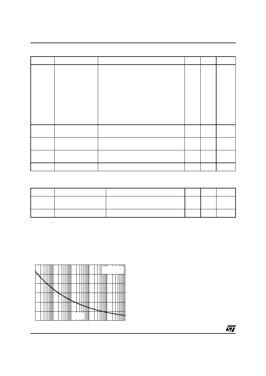
Fig 1 : Topology of the classical line card protection.
APPLICATION INFORMATION
Fig 2 : Classical use of the SSRP130B1.
The classical line card requires protection before
the ring relay and a second one for the SLIC (fig.1).
The use of new SLICs with integrated ring
generator or board based on solid state ring relay
suppresses this second protection (Fig. 2). Then
the only remaining stage, located between the line
and the ring relay, has to optimize the protection.
The classical symmetrical first stage protector
becomes not sufficient to avoid any circuit
destruction during surges.
The SSRP130B1 device takes into account this
fact and is based on asymmetrical voltage
characteristics (Fig.3a). The ring signal being
shifted back by the battery voltage, the
SSRP130B1 negative breakover value Vbo- is
greater than the positive one Vbo+. This point
guarantees a protection operation very close to the
peak of the normal operating voltage without any
disturbance of the ring signal.
Fig 3 : SSRP130B1 electrical characteristics.
I
V
Vbo-
Vbo+
a : Line to ground characteristics.
V
BR
-
V
BR
-
-
b : Line to line characteristics.
In addition with the 2 crowbar functions which
perform the protection of both TIP and RING lines
versus ground, a third cell assumes the differential
mode protection of the SLIC. The breakdown
voltage values of this third cell are the same for
both positive and negative parts of the
characteristics and are equivalent to the negative
breakdown voltage value of the TIP and RING
lines versus GND cells (Fig.3 b).
PTC
PTC
R
R
SLIC
SSRP130B1
Tip
Ring
(*)
(*) SLIC with integrated ring generator or solid state relay.
LINE
1st
stage
2nd
stage
PTC
PTC
R
R
SLIC
Ring generator
Line
Tip
Ring
SSRP130B1
2/7

Symbol
Parameter
Value
Unit
I
PP
Peak pulse current (see note 1)
10/1000
µ
s
5/310
µ
s
1/20
µ
s
2/10
µ
s
2x15
2x25
2x35
2x70
A
I
TSM
Non repetitive surge peak on-state current
(F=50Hz)
tp = 0.2 s
tp = 5 s
tp = 900 s
7.5
4.0
1.5
A
T
op
Operating temperature range
0 to + 70
°C
T
stg
T
j
Storage temperature range
Maximum operating junction temperature
- 55 to + 150
+ 150
°C
°C
T
L
Maximum lead temperature for soldering during 10s
260
°C
ABSOLUTE MAXIMUM RATINGS (T
amb
= 25
°
C)
Note 1 : Pulse waveform :
10/1000
µ
s
t
r
=10
µ
s
t
p
=1000
µ
s
5/310
µ
s
t
r
=5
µ
s
t
p
=310
µ
s
1/20
µ
s
t
r
=1
µ
s
t
p
=20
µ
s
2/10
µ
s
t
r
=2
µ
s
t
p
=10
µ
s
100
50
% I
PP
t
t
r
p
0
t
Symbol
Parameter
Value
Unit
R
th (j-a)
Junction to ambient
170
°
C/W
THERMAL RESISTANCE
V
I
I
H
I
BO
V
R
V
BR
BO
V
PP
I
R
I
Symbol
Parameter
V
R
Stand-off voltage
I
R
Leakage current at stand-off voltage
V
BR
Breakdown voltage
V
BO
Breakover voltage
I
H
Holding current
I
BO
Breakover current
I
PP
Peak pulse current
C
Capacitance
ELECTRICAL CHARACTERISTICS (T
amb
= 25°C)
SSRP130B1
3/7
Symbol
Parameter
Test conditions (note 1)
Min
Max
Unit
V
BO
Breakover voltage
(note 2)
Positive voltage
Negative voltage
50Hz
10/700
µ
s
1.2/50
µ
s
2/10
µ
s
50Hz
10/700
µ
s
1.2/50
µ
s
2/10
µ
s
200
175
180
250
280
235
240
340
V
I
BO
Breakover current
Positive voltage
Negative voltage
110
110
mA
I
H
Holding current
Positive polarity
Negative polarity
150
150
mA
I
R
Leakage current
(note 3)
V
R
= +130 V
V
R
= - 185 V
10
10
µ
A
C
Capacitance
F = 100kHz, V = 100mV, V
R
= 0V
100
pF
ELECTRICAL CHARACTERISTICS between TIP and GND, RING and GND (T
amb
=25°C)
Symbol
Parameter
Test conditions
Min
Max
Unit
I
R
Leakage current
(note 3)
V
R
= +185 V
V
R
= - 185 V
10
10
µ
A
C
Capacitance
F = 100kHz, V = 100mV, V
R
= 0V
100
pF
Note 1 :
Positive voltage means between T and G, or between R and G
Negative voltage means between G and T, or between G and T
Note 2 :
See test circuit for V
BO
parameters
Note 3 :
I
R
measured at V
R
guarantees V
BR
> V
R
ELECTRICAL CHARACTERISTICS between TIP and RING (T
am
b=25°C)
0.01
0.1
1
10
100
1000
5
10
15
I
(A)
TSM
F=50Hz
Tj initial=25°C
t(s)
Fig. 4 : Surge peak current versus overload
duration (maximum values).
SSRP130B1
4/7
FUNCTION HOLDING CURRENT (I
H
) TEST CIRCUIT (GO-NO GO TEST)
R
- V
P
V
BAT
= - 48 V
Surge generator
D.U.T.
This is a GO-NOGO test which allows to confirm the holding current (I
H
) level in a functional
test circuit.
TEST PROCEDURE :
1) Adjust the current level at the IH value by short circuiting the D.U.T.
2) Fire the D.U.T with a surge Current : Ipp = 10A , 10/1000 ms.
3) The D.U.T will come back off-state within 50 ms max.
Pulse (
µ
s)
V
p
C
1
C
2
L
R
1
R
2
R
3
R
4
I
PP
R
p
t
r
t
p
(V)
(
µ
F)
(nF)
(
µ
H)
(
)
(
)
(
)
(
)
(A)
(
)
10
700
1000
20
200
0
50
15
25
25
25
0
1.2
50
1500
1
33
0
76
13
25
25
30
10
2
10
2500
10
0
1.1
1.3
0
3
3
38
62
TEST CIRCUIT FOR V
BO
parameters :
C
C
R
R
TIP
RING
G ND
V
P
4
3
2
R
2
R
1
(V is defined in unload condition)
P
L
1
SSRP130B1
5/7