SGSIF344FP
HIGH VOLTAGE FAST-SWITCHING
NPN POWER TRANSISTOR
s
STMicroelectronics PREFERRED
SALESTYPE
s
HIGH VOLTAGE CAPABILITY
s
VERY HIGH SWITCHING SPEED
s
LOW BASE-DRIVE REQUIREMENTS
APPLICATIONS:
s
SWITCH MODE POWER SUPPLIES
s
HORIZONTAL DEFLECTION FOR COLOUR
TVS AND MONITORS
DESCRIPTION
The device is manufactured using Multiepitaxial
Mesa
technology
for
cost-effective
high
performance and uses a Hollow Emitter structure
to enhance switching speeds.
It
is
designed
for
high
speed
switching
applications
such
as
power
supplies
and
horizontal deflection circuits in TVs and monitors.
®
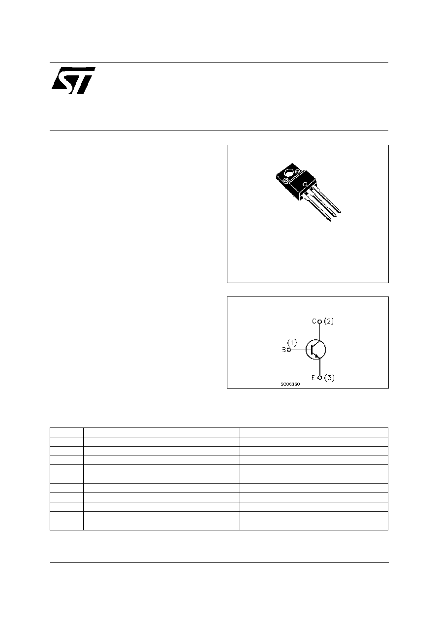
INTERNAL SCHEMATIC DIAGRAM
February 1999
ABSOLUTE MAXIMUM RATINGS
Symb ol
Parameter
Valu e
Un it
V
CES
Collect or-Emitter Volt age (V
BE
= 0)
1200
V
V
CEO
Collect or-Emitter Volt age (I
B
= 0)
600
V
V
EBO
Emitter-Base Volt age (I
C
= 0)
7
V
I
C
Collect or Current
7
A
I
CM
Collect or Peak Current (t
p
< 5 ms)
12
A
I
B
Base Current
5
A
I
BM
Base Peak Current (t
p
< 5 ms)
8
A
P
tot
T otal Dissipation at T
c
= 25
o
C
40
W
T
s tg
Storage Temperature
-65 to 150
o
C
T
j
Max. Operating Junction T emperature
150
o
C
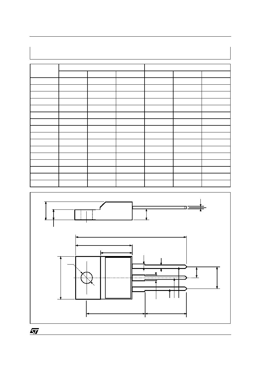
TO-220FP
1
2
3
1/6
THERMAL DATA
R
t hj-ca se
Thermal Resistance Junction-case
Max
3. 12
o
C/W
ELECTRICAL CHARACTERISTICS (T
case
= 25
o
C unless otherwise specified)
Symb ol
Parameter
Test Cond ition s
Mi n.
Typ .
Max.
Un it
I
CES
Collect or Cut-off
Current (V
BE
= 0)
V
CE
= 1200 V
200
µ
A
I
CEO
Collect or Cut-off
Current (I
B
= 0)
V
EC
= 380 V
V
EC
= 600 V
200
2
µ
A
mA
I
EBO
Emitt er Cut-off Current
(I
C
= 0)
V
BE
= 7 V
1
mA
V
CEO(sus )
Collect or-Emitter
Sustaining Voltage
I
C
= 100 mA
600
V
V
CE(sat )
Collect or-Emitter
Saturat ion Voltage
I
C
= 3. 5 A
I
B
= 0.7 A
I
C
= 2. 5 A
I
B
= 0.35 A
1.5
1.5
V
V
V
BE(s at)
Base-Emitt er
Saturat ion Voltage
I
C
= 3. 5 A
I
B
= 0.7 A
I
C
= 2. 5 A
I
B
= 0.35 A
1.5
1.5
V
V
t
on
t
s
t
f
RESI STIVE LO AD
Turn-on T ime
St orage Time
Fall T ime
V
CC
= 250 V
I
C
= 3.5 A
I
B1
= 0.7 A
I
B1
= -1.4 A
0.7
2.2
0. 18
1.2
3.5
0.4
µ
s
µ
s
µ
s
t
on
t
s
t
f
RESI STIVE LO AD
Turn-on T ime
St orage Time
Fall T ime
V
CC
= 250 V
I
C
= 3.5 A
I
B1
= 0.7 A
I
B1
= -1.4 A
With Ant isaturation Network
0.7
1.5
0.2
µ
s
µ
s
µ
s
t
on
t
s
t
f
RESI STIVE LO AD
Turn-on T ime
St orage Time
Fall T ime
V
CC
= 250 V
I
C
= 3.5 A
I
B1
= 0.7 A
V
BE(o ff
) = - 5 V
0.7
1
0.2
µ
s
µ
s
µ
s
t
s
t
f
INDUCTIVE LOAD
St orage Time
Fall T ime
I
C
= 3. 5 A
h
FE
= 5
V
CLAMP
= 450 V
V
BE(of f)
= -5 V
L = 300
µ
H
R
BB
= 1.2
1.4
0.1
2.8
0.2
µ
s
µ
s
t
s
t
f
INDUCTIVE LOAD
St orage Time
Fall T ime
I
C
= 3. 5 A
h
FE
= 5
V
CLAMP
= 450 V
V
BE(of f)
= -5 V
L = 300
µ
H
R
BB
= 1.2
T
c
= 100
o
C
4
0.3
µ
s
µ
s
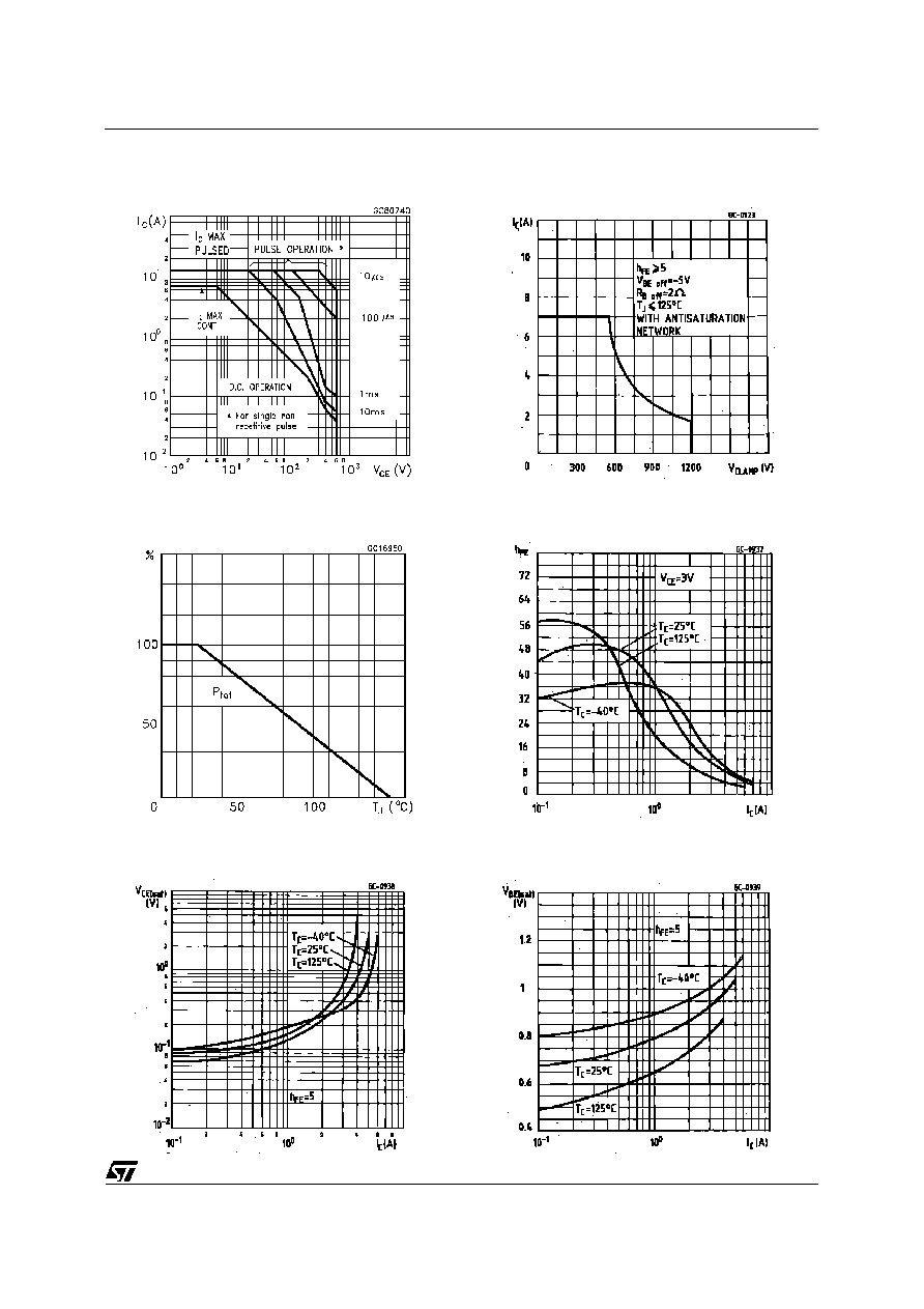
Pulsed: Pulse duration = 300
µ
s, duty cycle 1.5 %
SGSIF344FP
2/6
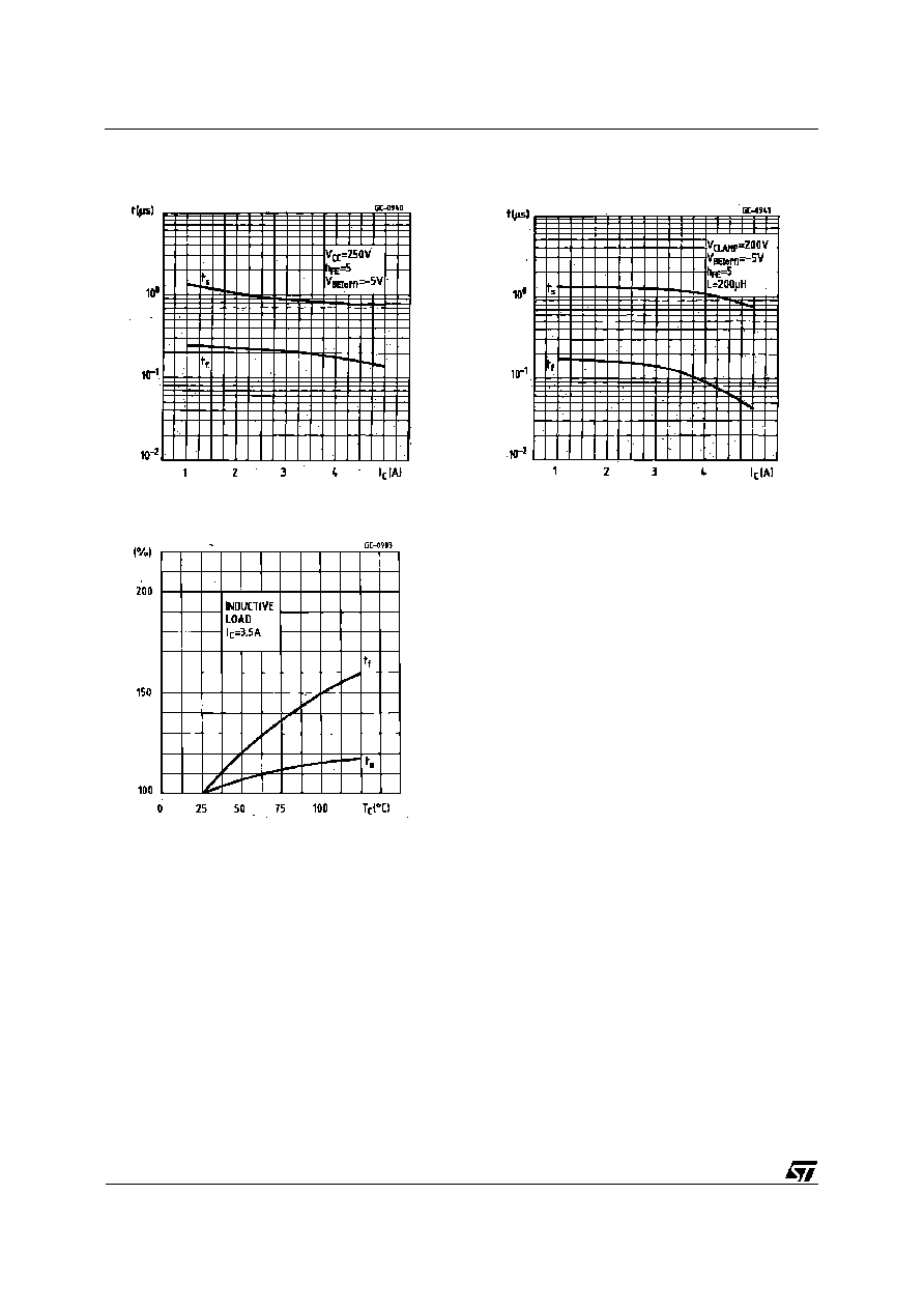
Resistive Load Switching Times
Inductive Load Switching Times
Switching Times Percentance Variation
SGSIF344FP
4/6