AVIONICS APPLICATIONS
RF & MICROWAVE TRANSISTORS
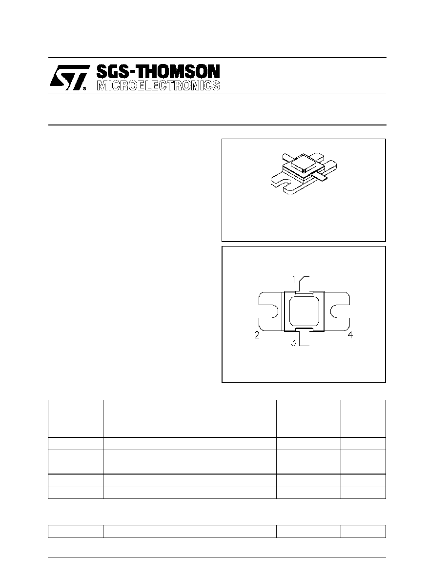
.400 x .400. 2LFL (M138)
hermetically sealed
DESCRIPTION
The SD1540-08 is a gold metallized silicon, NPN
power transistor designed for applications requiring
high peak power and low duty cycles such as
IFF, DME and TACAN. The SD1540 is packaged
in a metal/ceramic package with internal input/out-
put matching resulting in improved broadband per-
formance and a low thermal resistance.
PIN CONNECTION
BRANDING
SD1540-8
ORDER CODE
SD1540-08
ABSOLUTE MAXIMUM RATINGS (T
case
=
25
°
C)
Symbol
Parameter
Value
Uni t
V
CBO
Collector-Base Voltage
65
V
V
CES
Collector-Emitter Voltage
65
V
V
EBO
Emitter-Base Voltage
3.5
V
I
C
Device Current
22
A
P
DISS
Power Dissipation
875
W
T
J
Junction Temperature
+200
°
C
T
STG
Storage Temperature
-
65 to +150
°
C
R
TH(j-c)
Junction-Case Thermal Resistance
0.20
°
C/W
SD1540-08
1. Collector
3. Emitter
2. Base
4. Base
THERMAL DATA
November 1992
.
DESIGNED FOR HIGH POWER PULSED
IFF, DME, TACAN APPLICATIONS
.
350 WATTS (typ.) IFF 1030 - 1090 MHz
.
300 WATTS (min.) DME 1025 - 1150 MHz
.
290 WATTS (typ.) TACAN 960 - 1215 MHz
.
6.3 dB MIN. GAIN
.
REFRACTORY GOLD METALLIZATION
.
EMITTER BALLASTING AND LOW
THERMAL RESISTANCE FOR
RELIABILITY AND RUGGEDNESS
.
20:1 LOAD VSWR CAPABILITY AT
SPECIFIED OPERATING CONDITIONS
.
INPUT/OUTPUT MATCHED, COMMON
BASE CONFIGURATION
1/5

ELECTRICAL SPECIFICATIONS (T
case
=
25
°
C)
Symbol
Test Conditi ons
Value
Uni t
Min.
Typ.
Max.
P
OUT
f
=
1025 -- 1150MHz P
IN
=
70 W
V
CE
=
50 V
300
--
--
W
G
P
f
=
1025 -- 1150MHz P
IN
=
70 W
V
CE
=
50 V
6.3
--
--
dB
C
f
=
1025 -- 1150MHz P
IN
=
70 W
V
CE
=
50 V
35
--
--
%
N ote:
Pulse W idth
=
10
µ
Sec, Duty Cycle
=
1%
This device i s sui table f or use under other pulse widt h/duty cycle condit ions.
Please contact the fact ory for specific appli cat ions assi stance.
STATIC
Symbol
Test Conditions
Value
Unit
Min.
Typ.
Max.
BV
CBO
I
C
=
10mA
I
E
=
0mA
65
--
--
V
BV
CES
I
C
=
25mA
V
BE
=
0V
65
--
--
V
BV
EBO
I
E
=
5mA
I
C
=
0mA
3.5
--
--
V
I
CES
V
CE
=
50V
I
E
=
0mA
--
--
25
mA
h
FE
V
CE
=
5V
I
C
=
1A
10
--
--
--
DYNAMIC
TYPICAL PERFORMANCE
POWER OUTPUT vs POWER INPUT
POWER OUTPUT vs FREQUENCY
SD1540-08
2/5
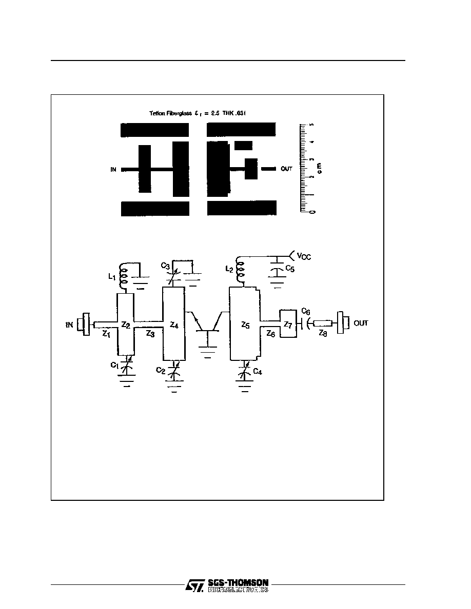
TYPICAL INPUT IMPEDANCE
TYPICAL COLLECTOR LOAD
IMPEDANCE
IMPEDANCE DATA
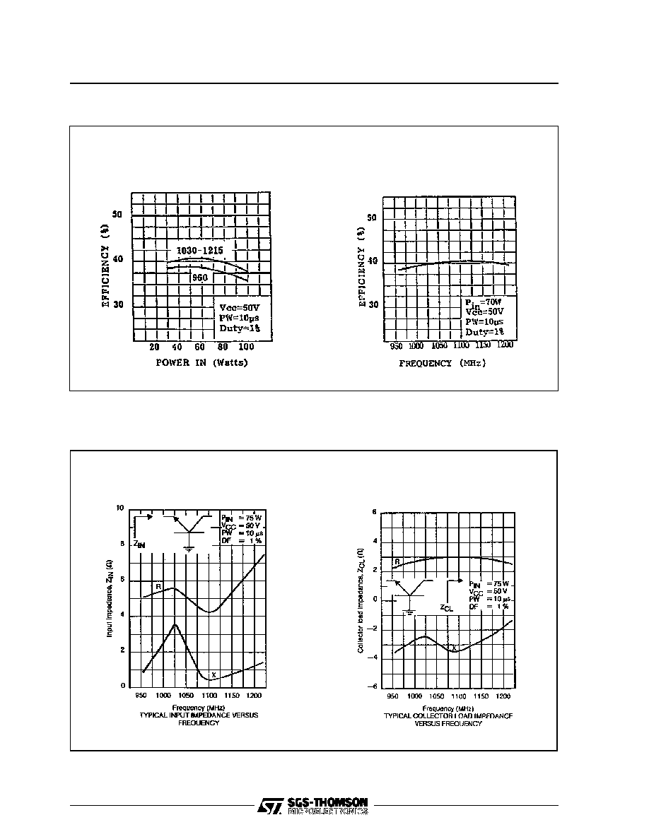
EFFICIENCY vs POWER INPUT
EFFICIENCY vs FREQUENCY
TYPICAL PERFORMANCE (cont'd)
SD1540-08
3/5
C1,C2.
C3, C4 : .6 - 4.5pF JOHANSON Gigatrim
C5
: 1000
µ
F, 63V, Electrolytic
C6
: 100pF Chip Capacitor Across .090 Gap
L1
: 2 Turns #24 .12 I.D., Spaced Wire Diameter
L2
: 4 Turns #24, .07 I.D., Spaced Wire Diameter
Z1
: .404 x .075
Z2
: .263 x .995
Z3
: .483 x .077
Z4
: .350 x 1.203
Z5
: .505 x 1.200 with Two Notches .05 Long
By .068 Wide
Z6
: .335 x .076
Z7
: .260 x .442
Z8
: .310 x .082
All Dimension are in Inches
TEST CIRCUIT
SD1540-08
4/5
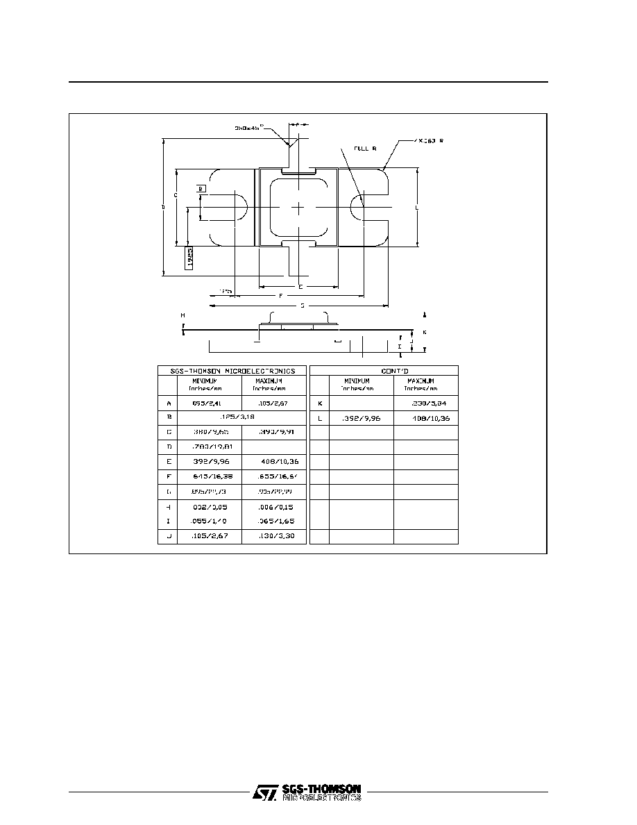
PACKAGE MECHANICAL DATA
Ref.: Dwg. No.12-0138
Information furnished is believed to be accurate and reliable. However, SGS-THOMSON Microelectronics assumes no responsability for the
consequences of use of such information nor for any infringement of patents or other rights of third parties which may results from its use. No
license is granted by implication or otherwise under any patent or patent rights of SGS-THOMSON Microelectronics. Specifications mentioned
in this publication are subject to change without notice. This publication supersedes and replaces all information previously supplied.
SGS-THOMSON Microelectronics products are not authorized for use as critical components in life support devices or systems without express
written approval of SGS-THOMSON Microelectonics.
©
1994 SGS-THOMSON Microelectronics - All Rights Reserved
SGS-THOMSON Microelectronics GROUP OF COMPANIES
Australia - Brazil - France - Germany - Hong Kong - Italy - Japan - Korea - Malaysia - Malta - Morocco - The Netherlands -
Singapore - Spain - Sweden - Switzerland - Taiwan - Thailand - United Kingdom - U.S.A
SD1540-08
5/5