Document Outline
- FEATURES SUMMARY
- SUMMARY DESCRIPTION
- SIGNAL DESCRIPTION
- CONNECTING TO THE SPI BUS
- OPERATING FEATURES
- MEMORY ORGANIZATION
- INSTRUCTIONS
- POWER-UP AND DELIVERY STATE
- INITIAL DELIVERY STATE
- MAXIMUM RATING
- DC AND AC PARAMETERS
- PACKAGE MECHANICAL
- Figure 19. PDIP8 … 8 pin Plastic DIP, 0.25mm lead frame, Package Outline
- Table 28. PDIP8 … 8 pin Plastic DIP, 0.25mm lead frame, Package Mechanical Data
- Figure 20. SO8 narrow … 8 lead Plastic Small Outline, 150 mils body width, Package Outline
- Table 29. SO8 narrow … 8 lead Plastic Small Outline, 150 mils body width, Package Mechanical Data
- Figure 21. TSSOP8 … 8 lead Thin Shrink Small Outline, Package Outline
- Table 30. TSSOP8 … 8 lead Thin Shrink Small Outline, Package Mechanical Data
- Figure 22. MLP8 - 8-lead Ultra thin Fine pitch Dual Flat No Lead, Package Outline
- Table 31. MLP8 - 8-lead Ultra thin Fine pitch Dual Flat No Lead, Package Mechanical Data
- PART NUMBERING
- REVISION HISTORY

1/42
May 2005
M95320 M95320-W M95320-R M95320-S
M95640 M95640-W M95640-R M95640-S
32Kbit and 64Kbit Serial SPI Bus EEPROMs
With High Speed Clock
FEATURES SUMMARY
Compatible with SPI Bus Serial Interface
(Positive Clock SPI Modes)
Single Supply Voltage:
4.5 to 5.5V for M95320 and M95640
2.5 to 5.5V for M95320-W and M95320-W
1.8 to 5.5V for M95320-R and M95640-R
1.65 to 5.5V for M95320-S and M95640-S
20MHz, 10MHz, 5MHz or 2MHz clock rates
5ms or 10ms Write Time
Status Register
Hardware Protection of the Status Register
BYTE and PAGE WRITE (up to 32 Bytes)
Self-Timed Programming Cycle
Adjustable Size Read-Only EEPROM Area
Enhanced ESD Protection
More than 100000 or 1 million Erase/Write
Cycles (depending on ordering options)
More than 40-Year Data Retention
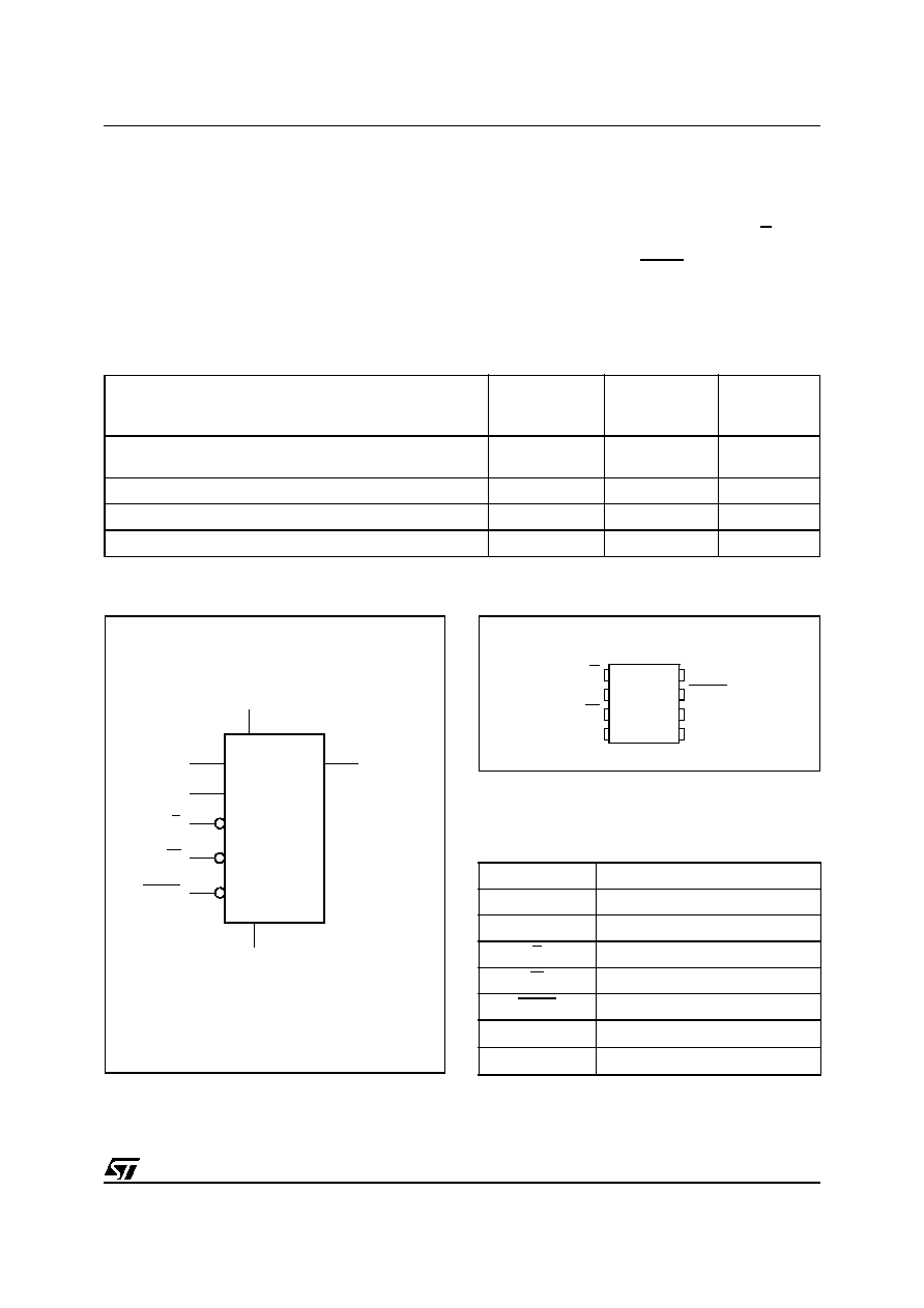
Table 1. Product List
Figure 1. Packages
Reference
Part Number
M95320
M95320
M95320-W
M95320-R
M95320-S
M95640
M95640
M95640-W
M95640-R
M95640-S
8
1
8
1
PDIP8 (BN)
0.25 mm frame
SO8 (MN)
150 mil width
TSSOP8 (DW)
169 mil width
MLP8 (MB)
2x3 mm

M95640, M95320
2/42
TABLE OF CONTENTS
FEATURES SUMMARY . . . . . . . . . . . . . . . . . . . . . . . . . . . . . . . . . . . . . . . . . . . . . . . . . . . . . . . . . . . . . 1
Table 1. Product List . . . . . . . . . . . . . . . . . . . . . . . . . . . . . . . . . . . . . . . . . . . . . . . . . . . . . . . . . . . . 1
Figure 1. Packages . . . . . . . . . . . . . . . . . . . . . . . . . . . . . . . . . . . . . . . . . . . . . . . . . . . . . . . . . . . . . . 1
SUMMARY DESCRIPTION . . . . . . . . . . . . . . . . . . . . . . . . . . . . . . . . . . . . . . . . . . . . . . . . . . . . . . . . . . . 5
Table 2. How to Identify Previous, Current and New Products by the Process Identification Letter 5
Figure 2. Logic Diagram . . . . . . . . . . . . . . . . . . . . . . . . . . . . . . . . . . . . . . . . . . . . . . . . . . . . . . . . . . 5
Figure 3. 8 Pin Package Connections. . . . . . . . . . . . . . . . . . . . . . . . . . . . . . . . . . . . . . . . . . . . . . . . 5
Table 3. Signal Names . . . . . . . . . . . . . . . . . . . . . . . . . . . . . . . . . . . . . . . . . . . . . . . . . . . . . . . . . . 5
SIGNAL DESCRIPTION . . . . . . . . . . . . . . . . . . . . . . . . . . . . . . . . . . . . . . . . . . . . . . . . . . . . . . . . . . . . . 6
Serial Data Output (Q) . . . . . . . . . . . . . . . . . . . . . . . . . . . . . . . . . . . . . . . . . . . . . . . . . . . . . . . . . . . . 6
Serial Data Input (D) . . . . . . . . . . . . . . . . . . . . . . . . . . . . . . . . . . . . . . . . . . . . . . . . . . . . . . . . . . . . . 6
Serial Clock (C) . . . . . . . . . . . . . . . . . . . . . . . . . . . . . . . . . . . . . . . . . . . . . . . . . . . . . . . . . . . . . . . . . 6
Chip Select (S) . . . . . . . . . . . . . . . . . . . . . . . . . . . . . . . . . . . . . . . . . . . . . . . . . . . . . . . . . . . . . . . . . 6
Hold (HOLD) . . . . . . . . . . . . . . . . . . . . . . . . . . . . . . . . . . . . . . . . . . . . . . . . . . . . . . . . . . . . . . . . . . . 6
Write Protect (W) . . . . . . . . . . . . . . . . . . . . . . . . . . . . . . . . . . . . . . . . . . . . . . . . . . . . . . . . . . . . . . . . 6
CONNECTING TO THE SPI BUS . . . . . . . . . . . . . . . . . . . . . . . . . . . . . . . . . . . . . . . . . . . . . . . . . . . . . . 7
Figure 4. Bus Master and Memory Devices on the SPI Bus. . . . . . . . . . . . . . . . . . . . . . . . . . . . . . . 7
SPI Modes . . . . . . . . . . . . . . . . . . . . . . . . . . . . . . . . . . . . . . . . . . . . . . . . . . . . . . . . . . . . . . . . . . . . 8
Figure 5. SPI Modes Supported . . . . . . . . . . . . . . . . . . . . . . . . . . . . . . . . . . . . . . . . . . . . . . . . . . . . 8
OPERATING FEATURES . . . . . . . . . . . . . . . . . . . . . . . . . . . . . . . . . . . . . . . . . . . . . . . . . . . . . . . . . . . . 9
Power-Up . . . . . . . . . . . . . . . . . . . . . . . . . . . . . . . . . . . . . . . . . . . . . . . . . . . . . . . . . . . . . . . . . . . . . 9
. . . . . . . . . . . . . . . . . . . . . . . . . . . . . . . . . . . . . . . . . . . . . . . . . . . . . . . . . . . . . . . . . . . . . . . . . . . . . . 9
Power On Reset: VCC Lock-Out Write Protect . . . . . . . . . . . . . . . . . . . . . . . . . . . . . . . . . . . . . . . 9
Power-down . . . . . . . . . . . . . . . . . . . . . . . . . . . . . . . . . . . . . . . . . . . . . . . . . . . . . . . . . . . . . . . . . . . 9
Active Power and Standby Power Modes . . . . . . . . . . . . . . . . . . . . . . . . . . . . . . . . . . . . . . . . . . . 9
Hold Condition . . . . . . . . . . . . . . . . . . . . . . . . . . . . . . . . . . . . . . . . . . . . . . . . . . . . . . . . . . . . . . . . . 9
Figure 6. Hold Condition Activation. . . . . . . . . . . . . . . . . . . . . . . . . . . . . . . . . . . . . . . . . . . . . . . . . 10
. . . . . . . . . . . . . . . . . . . . . . . . . . . . . . . . . . . . . . . . . . . . . . . . . . . . . . . . . . . . . . . . . . . . . . . . . . . . . 10
Status Register . . . . . . . . . . . . . . . . . . . . . . . . . . . . . . . . . . . . . . . . . . . . . . . . . . . . . . . . . . . . . . . 10
WIP bit . . . . . . . . . . . . . . . . . . . . . . . . . . . . . . . . . . . . . . . . . . . . . . . . . . . . . . . . . . . . . . . . . . . . . . . 10
WEL bit . . . . . . . . . . . . . . . . . . . . . . . . . . . . . . . . . . . . . . . . . . . . . . . . . . . . . . . . . . . . . . . . . . . . . . 10
BP1, BP0 bits . . . . . . . . . . . . . . . . . . . . . . . . . . . . . . . . . . . . . . . . . . . . . . . . . . . . . . . . . . . . . . . . . 10
SRWD bit . . . . . . . . . . . . . . . . . . . . . . . . . . . . . . . . . . . . . . . . . . . . . . . . . . . . . . . . . . . . . . . . . . . . . 10
Table 4. Status Register Format . . . . . . . . . . . . . . . . . . . . . . . . . . . . . . . . . . . . . . . . . . . . . . . . . . 10
. . . . . . . . . . . . . . . . . . . . . . . . . . . . . . . . . . . . . . . . . . . . . . . . . . . . . . . . . . . . . . . . . . . . . . . . . . . . . 10
Data Protection and Protocol Control . . . . . . . . . . . . . . . . . . . . . . . . . . . . . . . . . . . . . . . . . . . . . 10
Table 5. Write-Protected Block Size . . . . . . . . . . . . . . . . . . . . . . . . . . . . . . . . . . . . . . . . . . . . . . . 11
MEMORY ORGANIZATION . . . . . . . . . . . . . . . . . . . . . . . . . . . . . . . . . . . . . . . . . . . . . . . . . . . . . . . . . 12

3/42
M95640, M95320
Figure 7. Block Diagram . . . . . . . . . . . . . . . . . . . . . . . . . . . . . . . . . . . . . . . . . . . . . . . . . . . . . . . . . 12
INSTRUCTIONS . . . . . . . . . . . . . . . . . . . . . . . . . . . . . . . . . . . . . . . . . . . . . . . . . . . . . . . . . . . . . . . . . . 13
Table 6. Instruction Set . . . . . . . . . . . . . . . . . . . . . . . . . . . . . . . . . . . . . . . . . . . . . . . . . . . . . . . . . 13
Write Enable (WREN) . . . . . . . . . . . . . . . . . . . . . . . . . . . . . . . . . . . . . . . . . . . . . . . . . . . . . . . . . . 14
Figure 8. Write Enable (WREN) Sequence. . . . . . . . . . . . . . . . . . . . . . . . . . . . . . . . . . . . . . . . . . . 14
Write Disable (WRDI) . . . . . . . . . . . . . . . . . . . . . . . . . . . . . . . . . . . . . . . . . . . . . . . . . . . . . . . . . . . 14
Figure 9. Write Disable (WRDI) Sequence . . . . . . . . . . . . . . . . . . . . . . . . . . . . . . . . . . . . . . . . . . . 14
Read Status Register (RDSR) . . . . . . . . . . . . . . . . . . . . . . . . . . . . . . . . . . . . . . . . . . . . . . . . . . . . 15
WIP bit . . . . . . . . . . . . . . . . . . . . . . . . . . . . . . . . . . . . . . . . . . . . . . . . . . . . . . . . . . . . . . . . . . . . . . . 15
WEL bit . . . . . . . . . . . . . . . . . . . . . . . . . . . . . . . . . . . . . . . . . . . . . . . . . . . . . . . . . . . . . . . . . . . . . . 15
BP1, BP0 bits . . . . . . . . . . . . . . . . . . . . . . . . . . . . . . . . . . . . . . . . . . . . . . . . . . . . . . . . . . . . . . . . . 15
SRWD bit . . . . . . . . . . . . . . . . . . . . . . . . . . . . . . . . . . . . . . . . . . . . . . . . . . . . . . . . . . . . . . . . . . . . . 15
Figure 10.Read Status Register (RDSR) Sequence . . . . . . . . . . . . . . . . . . . . . . . . . . . . . . . . . . . . 15
Write Status Register (WRSR) . . . . . . . . . . . . . . . . . . . . . . . . . . . . . . . . . . . . . . . . . . . . . . . . . . . 16
Table 7. Protection Modes. . . . . . . . . . . . . . . . . . . . . . . . . . . . . . . . . . . . . . . . . . . . . . . . . . . . . . . 16
Table 8. Address Range Bits . . . . . . . . . . . . . . . . . . . . . . . . . . . . . . . . . . . . . . . . . . . . . . . . . . . . . 17
Figure 11.Write Status Register (WRSR) Sequence . . . . . . . . . . . . . . . . . . . . . . . . . . . . . . . . . . . . 17
Read from Memory Array (READ) . . . . . . . . . . . . . . . . . . . . . . . . . . . . . . . . . . . . . . . . . . . . . . . . 18
Figure 12.Read from Memory Array (READ) Sequence . . . . . . . . . . . . . . . . . . . . . . . . . . . . . . . . . 18
Write to Memory Array (WRITE) . . . . . . . . . . . . . . . . . . . . . . . . . . . . . . . . . . . . . . . . . . . . . . . . . . 19
Figure 13.Byte Write (WRITE) Sequence . . . . . . . . . . . . . . . . . . . . . . . . . . . . . . . . . . . . . . . . . . . . 19
Figure 14.Page Write (WRITE) Sequence . . . . . . . . . . . . . . . . . . . . . . . . . . . . . . . . . . . . . . . . . . . 20
POWER-UP AND DELIVERY STATE. . . . . . . . . . . . . . . . . . . . . . . . . . . . . . . . . . . . . . . . . . . . . . . . . . 21
Power-up State . . . . . . . . . . . . . . . . . . . . . . . . . . . . . . . . . . . . . . . . . . . . . . . . . . . . . . . . . . . . . . . 21
INITIAL DELIVERY STATE. . . . . . . . . . . . . . . . . . . . . . . . . . . . . . . . . . . . . . . . . . . . . . . . . . . . . . . . . . 21
MAXIMUM RATING. . . . . . . . . . . . . . . . . . . . . . . . . . . . . . . . . . . . . . . . . . . . . . . . . . . . . . . . . . . . . . . . 22
Table 9. Absolute Maximum Ratings . . . . . . . . . . . . . . . . . . . . . . . . . . . . . . . . . . . . . . . . . . . . . . . 22
DC AND AC PARAMETERS. . . . . . . . . . . . . . . . . . . . . . . . . . . . . . . . . . . . . . . . . . . . . . . . . . . . . . . . . 23
Table 10. Operating Conditions (M95320 and M95640) . . . . . . . . . . . . . . . . . . . . . . . . . . . . . . . . . 23
Table 11. Operating Conditions (M95320-W and M95640-W) . . . . . . . . . . . . . . . . . . . . . . . . . . . . 23
Table 12. Operating Conditions (M95320-R and M95640-R) . . . . . . . . . . . . . . . . . . . . . . . . . . . . . 23
Table 13. Operating Conditions (M95320-S and M95640-S) . . . . . . . . . . . . . . . . . . . . . . . . . . . . . 23
Table 14. AC Measurement Conditions. . . . . . . . . . . . . . . . . . . . . . . . . . . . . . . . . . . . . . . . . . . . . . 23
Figure 15.AC Measurement I/O Waveform . . . . . . . . . . . . . . . . . . . . . . . . . . . . . . . . . . . . . . . . . . . 24
Table 15. Capacitance. . . . . . . . . . . . . . . . . . . . . . . . . . . . . . . . . . . . . . . . . . . . . . . . . . . . . . . . . . . 24
Table 16. DC Characteristics (M95320 and M95640, Device Grade 6) . . . . . . . . . . . . . . . . . . . . . 24
Table 17. DC Characteristics (M95320 and M95640, Device Grade 3) . . . . . . . . . . . . . . . . . . . . . 25
Table 18. DC Characteristics (M95320-W and M95640-W, Device Grade 6) . . . . . . . . . . . . . . . . . 26
Table 19. DC Characteristics (M95320-W and M95640-W, Device Grade 3) . . . . . . . . . . . . . . . . . 27
Table 20. DC Characteristics (M95320-R and M95640-R) . . . . . . . . . . . . . . . . . . . . . . . . . . . . . . . 27
Table 21. DC Characteristics (M95320-S and M95640-S) . . . . . . . . . . . . . . . . . . . . . . . . . . . . . . . 27

M95640, M95320
4/42
Table 22. AC Characteristics (M95320 and M95640, Device Grade 6). . . . . . . . . . . . . . . . . . . . . . 28
Table 23. AC Characteristics (M95320 and M95640, Device Grade 3). . . . . . . . . . . . . . . . . . . . . . 29
Table 24. AC Characteristics (M95320-W and M95640-W, Device Grade 6) . . . . . . . . . . . . . . . . . 30
Table 25. AC Characteristics (M95320-W and M95640-W, Device Grade 3) . . . . . . . . . . . . . . . . . 31
Table 26. AC Characteristics (M95320-R and M95640-R) . . . . . . . . . . . . . . . . . . . . . . . . . . . . . . . 32
Table 27. AC Characteristics (M95320-S and M95640-S, Device Grade 3) . . . . . . . . . . . . . . . . . . 33
Figure 16.Serial Input Timing . . . . . . . . . . . . . . . . . . . . . . . . . . . . . . . . . . . . . . . . . . . . . . . . . . . . . 34
Figure 17.Hold Timing . . . . . . . . . . . . . . . . . . . . . . . . . . . . . . . . . . . . . . . . . . . . . . . . . . . . . . . . . . . 34
Figure 18.Output Timing . . . . . . . . . . . . . . . . . . . . . . . . . . . . . . . . . . . . . . . . . . . . . . . . . . . . . . . . . 35
PACKAGE MECHANICAL . . . . . . . . . . . . . . . . . . . . . . . . . . . . . . . . . . . . . . . . . . . . . . . . . . . . . . . . . . 36
Figure 19.PDIP8 8 pin Plastic DIP, 0.25mm lead frame, Package Outline . . . . . . . . . . . . . . . . . 36
Table 28. PDIP8 8 pin Plastic DIP, 0.25mm lead frame, Package Mechanical Data . . . . . . . . . . 36
Figure 20.SO8 narrow 8 lead Plastic Small Outline, 150 mils body width, Package Outline . . . . 37
Table 29. SO8 narrow 8 lead Plastic Small Outline, 150 mils body width, Package Mechanical Data
37
Figure 21.TSSOP8 8 lead Thin Shrink Small Outline, Package Outline . . . . . . . . . . . . . . . . . . . 38
Table 30. TSSOP8 8 lead Thin Shrink Small Outline, Package Mechanical Data . . . . . . . . . . . . 38
Figure 22.MLP8 - 8-lead Ultra thin Fine pitch Dual Flat No Lead, Package Outline . . . . . . . . . . . . 39
Table 31. MLP8 - 8-lead Ultra thin Fine pitch Dual Flat No Lead, Package Mechanical Data . . . . 39
PART NUMBERING . . . . . . . . . . . . . . . . . . . . . . . . . . . . . . . . . . . . . . . . . . . . . . . . . . . . . . . . . . . . . . . 40
Table 32. Ordering Information Scheme . . . . . . . . . . . . . . . . . . . . . . . . . . . . . . . . . . . . . . . . . . . . . 40
REVISION HISTORY . . . . . . . . . . . . . . . . . . . . . . . . . . . . . . . . . . . . . . . . . . . . . . . . . . . . . . . . . . . . . . . 41
Table 33. Document Revision History . . . . . . . . . . . . . . . . . . . . . . . . . . . . . . . . . . . . . . . . . . . . . . . 41
5/42
M95640, M95320
SUMMARY DESCRIPTION
These electrically erasable programmable memo-
ry (EEPROM) devices are accessed by a high
speed SPI-compatible bus.
The M95320, M95320-W, M95320-R and
M95320-S are 32Kbit devices organized as 4096
x 8 bits. The M95640, M95640-W, M95640-R and
M95640-S are 64Kbit devices organized as 8192
x 8 bits.
The device is accessed by a simple serial interface
that is SPI-compatible. The bus signals are C, D
and Q, as shown in
Table 3.
and
Figure 2.
.
The device is selected when Chip Select (S) is tak-
en Low. Communications with the device can be
interrupted using Hold (HOLD).
The devices are available in three different ver-
sions identified by a specific marking (see
Table
2.
).
Table 2. How to Identify Previous, Current and New Products by the Process Identification Letter
Note: 1. For further information, please ask your ST Sales Office for Process Change Notices.
Figure 2. Logic Diagram
Figure 3. 8 Pin Package Connections
Note: 1. See
PACKAGE MECHANICAL
section for package di-
mensions and how to identify pin-1.
2. NC, Not Connected.
Table 3. Signal Names
Devices Root Part Numbers
Markings on
Previous
Products
1
Markings on
Current
Products
1
Markings on
New
Products
1
M95320, M95640, M95320-W, M95640-W
Device Grade 6
xxxxS
xxxxV
xxxxP
M95320, M95640, M95320-W, M95640-W Device Grade 3
xxxxS
xxxxB
xxxxP
M95320-R, M95640-R
-
-
xxxxP
M95320-S, M95640-S
-
-
xxxxP
AI01789C
S
VCC
M95xxx
HOLD
VSS
W
Q
C
D
C
Serial Clock
D
Serial data Input
Q
Serial data Output
S
Chip Select
W
Write Protect
HOLD
Hold
V
CC
Supply Voltage
V
SS
Ground
D
VSS
C
HOLD
Q
S
VCC
W
AI01790D
M95xxx
1
2
3
4
8
7
6
5

M95640, M95320
6/42
SIGNAL DESCRIPTION
During all operations, V
CC
must be held stable and
within the specified valid range: V
CC
(min) to
V
CC
(max).
All of the input and output signals must be held
High or Low (according to voltages of V
IH
, V
OH
, V
IL
or V
OL
, as specified in
Table 16.
to
Table 20.
).
These signals are described next.
Serial Data Output (Q). This output signal is
used to transfer data serially out of the device.
Data is shifted out on the falling edge of Serial
Clock (C).
Serial Data Input (D). This input signal is used to
transfer data serially into the device. It receives in-
structions, addresses, and the data to be written.
Values are latched on the rising edge of Serial
Clock (C).
Serial Clock (C). This input signal provides the
timing of the serial interface. Instructions, address-
es, or data present at Serial Data Input (D) are
latched on the rising edge of Serial Clock (C). Data
on Serial Data Output (Q) changes after the falling
edge of Serial Clock (C).
Chip Select (S). When this input signal is High,
the device is deselected and Serial Data Output
(Q) is at high impedance. Unless an internal Write
cycle is in progress, the device will be in the Stand-
by Power mode. Driving Chip Select (S) Low se-
lects the device, placing it in the Active Power
mode.
After Power-up, a falling edge on Chip Select (S)
is required prior to the start of any instruction.
Hold (HOLD). The Hold (HOLD) signal is used to
pause any serial communications with the device
without deselecting the device.
During the Hold condition, the Serial Data Output
(Q) is high impedance, and Serial Data Input (D)
and Serial Clock (C) are Don't Care.
To start the Hold condition, the device must be se-
lected, with Chip Select (S) driven Low.
Write Protect (W). The main purpose of this in-
put signal is to freeze the size of the area of mem-
ory that is protected against Write instructions (as
specified by the values in the BP1 and BP0 bits of
the Status Register).
This pin must be driven either High or Low, and
must be stable during all write operations.

7/42
M95640, M95320
CONNECTING TO THE SPI BUS
These devices are fully compatible with the SPI
protocol.
All instructions, addresses and input data bytes
are shifted in to the device, most significant bit
first. The Serial Data Input (D) is sampled on the
first rising edge of the Serial Clock (C) after Chip
Select (S) goes Low.
All output data bytes are shifted out of the device,
most significant bit first. The Serial Data Output
(Q) is latched on the first falling edge of the Serial
Clock (C) after the instruction (such as the Read
from Memory Array and Read Status Register in-
structions) have been clocked into the device.
Figure 4.
shows three devices, connected to an
MCU, on a SPI bus. Only one device is selected at
a time, so only one device drives the Serial Data
Output (Q) line at a time, all the others being high
impedance.
Figure 4. Bus Master and Memory Devices on the SPI Bus
Note: The Write Protect (W) and Hold (HOLD) signals should be driven, High or Low as appropriate.
AI03746e
Bus Master
(ST6, ST7, ST9,
ST10, Others)
SPI Memory
Device
SDO
SDI
SCK
C
Q
D
S
SPI Memory
Device
C
Q
D
S
SPI Memory
Device
C
Q
D
S
CS3
CS2
CS1
SPI Interface with
(CPOL, CPHA) =
(0, 0) or (1, 1)
W
HOLD
W
HOLD
W
HOLD
R
R
R
V
CC
V
CC
V
CC
V
CC
M95640, M95320
8/42
SPI Modes
These devices can be driven by a microcontroller
with its SPI peripheral running in either of the two
following modes:
CPOL=0, CPHA=0
CPOL=1, CPHA=1
For these two modes, input data is latched in on
the rising edge of Serial Clock (C), and output data
is available from the falling edge of Serial Clock
(C).
The difference between the two modes, as shown
in
Figure 5.
, is the clock polarity when the bus
master is in Stand-by mode and not transferring
data:
C remains at 0 for (CPOL=0, CPHA=0)
C remains at 1 for (CPOL=1, CPHA=1)
Figure 5. SPI Modes Supported
AI01438B
C
MSB
CPHA
D
0
1
CPOL
0
1
Q
C
MSB

9/42
M95640, M95320
OPERATING FEATURES
Power-Up
When the power supply is turned on, V
CC
rises
from V
SS
to V
CC
.
During this time, the Chip Select (S) must be al-
lowed to follow the V
CC
voltage. It must not be al-
lowed to float, but should be connected to V
CC
via
a suitable pull-up resistor.
As a built in safety feature, Chip Select (S) is edge
sensitive as well as level sensitive. After Power-
up, the device does not become selected until a
falling edge has first been detected on Chip Select
(S). This ensures that Chip Select (S) must have
been High, prior to going Low to start the first op-
eration.
Power On Reset: V
CC
Lock-Out Write Protect
In order to prevent inadvertent Write operations
during Power-up, each device include a Power On
Reset (POR) circuit. At Power-up, the device will
not respond to any instruction until V
CC
has
reached the Power On Reset threshold voltage.
This threshold is lower than the V
CC
min operating
voltage defined in Tables
10
,
11
,
12
and
13
.
Similarly, as soon as V
CC
drops from the normal
operating voltage, below the Power On Reset
threshold voltage, the device stops responding to
any instruction sent to it.
Prior to selecting and issuing instructions to the
memory, a valid stable V
CC
voltage must be ap-
plied. This voltage must remain stable and valid
until the end of the transmission of the instruction
and, for a Write instruction, until the completion o
the internal write cycle (t
W
).
Power-down
At Power-down, the device must be deselected.
Chip Select (S) should be allowed to follow the
voltage applied on V
CC
.
Active Power and Standby Power Modes
When Chip Select (S) is Low, the device is select-
ed, and in the Active Power mode. The device
consumes I
CC
, as specified in
Table 16.
to
Table
20.
.
When Chip Select (S) is High, the device is dese-
lected. If an Erase/Write cycle is not currently in
progress, the device then goes in to the Standby
Power mode, and the device consumption drops
to I
CC1
.
Hold Condition
The Hold (HOLD) signal is used to pause any se-
rial communications with the device without reset-
ting the clocking sequence.
During the Hold condition, the Serial Data Output
(Q) is high impedance, and Serial Data Input (D)
and Serial Clock (C) are Don't Care.
To enter the Hold condition, the device must be
selected, with Chip Select (S) Low.
Normally, the device is kept selected, for the whole
duration of the Hold condition. Deselecting the de-
vice while it is in the Hold condition, has the effect
of resetting the state of the device, and this mech-
anism can be used if it is required to reset any pro-
cesses that had been in progress.
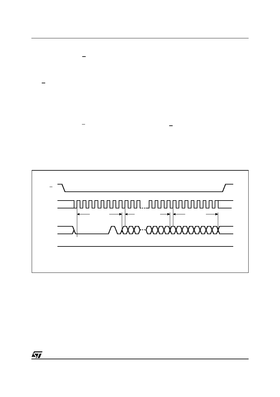
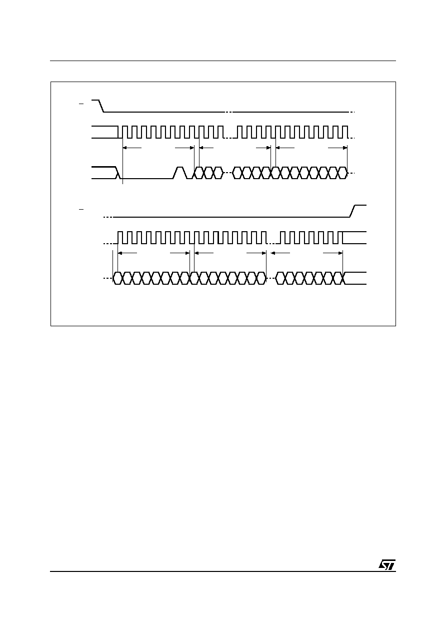
The Hold condition starts when the Hold (HOLD)
signal is driven Low at the same time as Serial
Clock (C) already being Low (as shown in
Figure
6.
).
The Hold condition ends when the Hold (HOLD)
signal is driven High at the same time as Serial
Clock (C) already being Low.
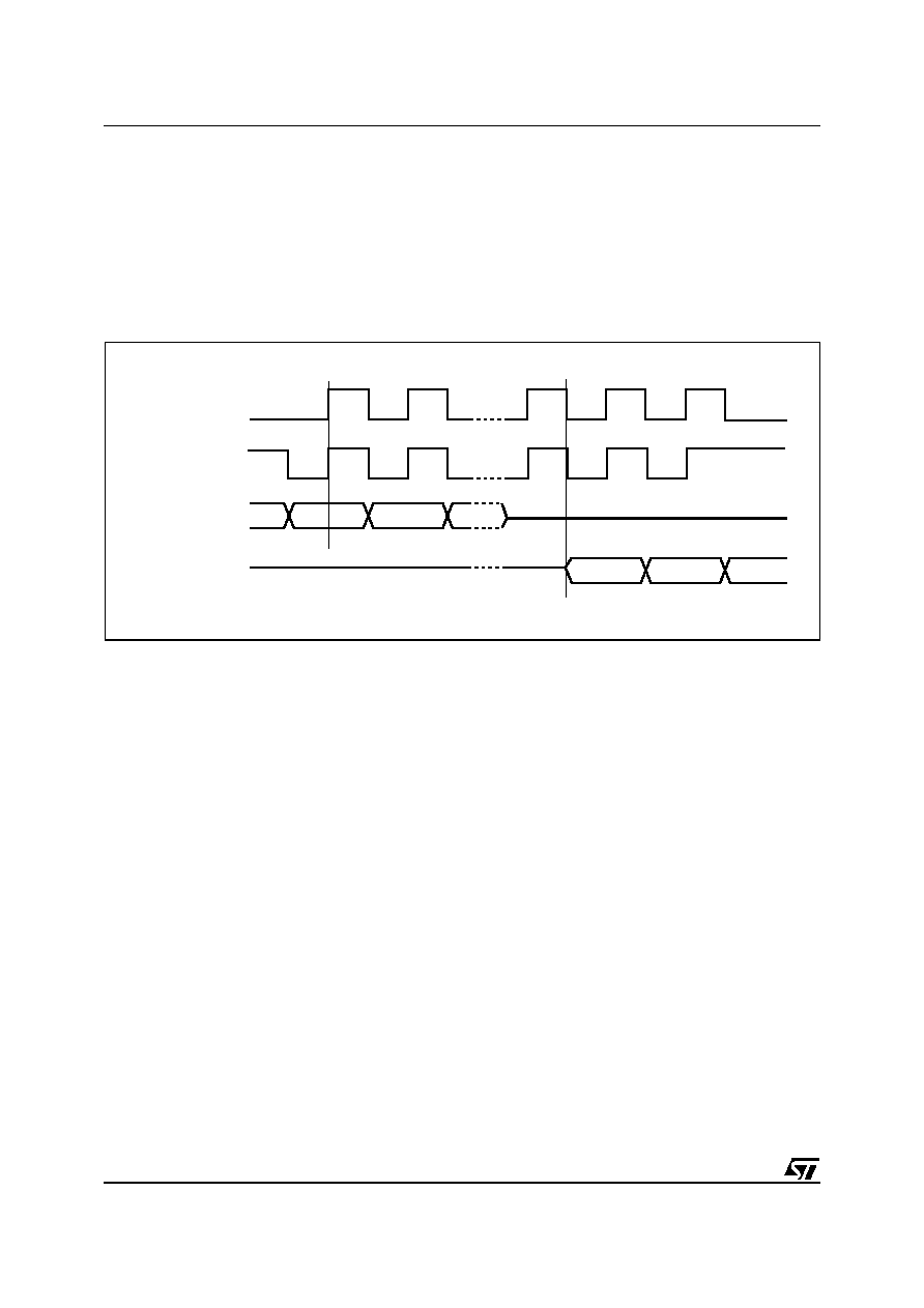
Figure 6.
also shows what happens if the rising
and falling edges are not timed to coincide with
Serial Clock (C) being Low.

M95640, M95320
10/42
Figure 6. Hold Condition Activation
Status Register
Figure 7.
shows the position of the Status Register
in the control logic of the device. The Status Reg-
ister contains a number of status and control bits
that can be read or set (as appropriate) by specific
instructions.
WIP bit. The Write In Progress (WIP) bit indicates
whether the memory is busy with a Write or Write
Status Register cycle.
WEL bit. The Write Enable Latch (WEL) bit indi-
cates the status of the internal Write Enable Latch.
BP1, BP0 bits. The Block Protect (BP1, BP0) bits
are non-volatile. They define the size of the area to
be software protected against Write instructions.
SRWD bit. The Status Register Write Disable
(SRWD) bit is operated in conjunction with the
Write Protect (W) signal. The Status Register
Write Disable (SRWD) bit and Write Protect (W)
signal allow the device to be put in the Hardware
Protected mode. In this mode, the non-volatile bits
of the Status Register (SRWD, BP1, BP0) become
read-only bits.
Table 4. Status Register Format
Data Protection and Protocol Control
Non-volatile memory devices can be used in envi-
ronments that are particularly noisy, and within ap-
plications that could experience problems if
memory bytes are corrupted. Consequently, the
device features the following data protection
mechanisms:
Write and Write Status Register instructions
are checked that they consist of a number of
clock pulses that is a multiple of eight, before
they are accepted for execution.
All instructions that modify data must be
preceded by a Write Enable (WREN)
instruction to set the Write Enable Latch
(WEL) bit. This bit is returned to its reset state
by the following events:
Power-up
Write Disable (WRDI) instruction
completion
Write Status Register (WRSR) instruction
completion
Write (WRITE) instruction completion
The Block Protect (BP1, BP0) bits allow part of
the memory to be configured as read-only.
This is the Software Protected Mode (SPM).
The Write Protect (W) signal allows the Block
Protect (BP1, BP0) bits to be protected. This is
the Hardware Protected Mode (HPM).
For any instruction to be accepted, and executed,
Chip Select (S) must be driven High after the rising
edge of Serial Clock (C) for the last bit of the in-
struction, and before the next rising edge of Serial
Clock (C).
Two points need to be noted in the previous sen-
tence:
AI02029D
HOLD
C
Hold
Condition
Hold
Condition
b7 b0
SRWD
0
0
0 BP1 BP0 WEL WIP
Status Register Write Protect
Block Protect Bits
Write Enable Latch Bit
Write In Progress Bit

11/42
M95640, M95320
The `last bit of the instruction' can be the
eighth bit of the instruction code, or the eighth
bit of a data byte, depending on the instruction
(except for Read Status Register (RDSR) and
Read (READ) instructions).
The `next rising edge of Serial Clock (C)' might
(or might not) be the next bus transaction for
some other device on the SPI bus.
Table 5. Write-Protected Block Size
Status Register Bits
Protected Block
Array Addresses Protected
BP1 BP0
M95640, M95640-W,
M95640-R, M95640-S
M95320, M95320-W,
M95320-R, M95320-S
0 0
none
none
none
0
1
Upper quarter
1800h - 1FFFh
0C00h - 0FFFh
1
0
Upper half
1000h - 1FFFh
0800h - 0FFFh
1
1
Whole memory
0000h - 1FFFh
0000h - 0FFFh

M95640, M95320
12/42
MEMORY ORGANIZATION
The memory is organized as shown in
Figure 7.
.
Figure 7. Block Diagram
AI01272C
HOLD
S
W
Control Logic
High Voltage
Generator
I/O Shift Register
Address Register
and Counter
Data
Register
1 Page
X Decoder
Y Decoder
C
D
Q
Size of the
Read only
EEPROM
area
Status
Register
13/42
M95640, M95320
INSTRUCTIONS
Each instruction starts with a single-byte code, as
summarized in
Table 6.
.
If an invalid instruction is sent (one not contained
in
Table 6.
), the device automatically deselects it-
self.
Table 6. Instruction Set
Instruc
tion
Description
Instruction
Format
WREN
Write Enable
0000 0110
WRDI
Write Disable
0000 0100
RDSR
Read Status Register
0000 0101
WRSR
Write Status Register
0000 0001
READ
Read from Memory Array
0000 0011
WRITE
Write to Memory Array
0000 0010

M95640, M95320
14/42
Write Enable (WREN)
The Write Enable Latch (WEL) bit must be set pri-
or to each WRITE and WRSR instruction. The only
way to do this is to send a Write Enable instruction
to the device.
As shown in
Figure 8.
, to send this instruction to
the device, Chip Select (S) is driven Low, and the
bits of the instruction byte are shifted in, on Serial
Data Input (D). The device then enters a wait
state. It waits for a the device to be deselected, by
Chip Select (S) being driven High.
Figure 8. Write Enable (WREN) Sequence
Write Disable (WRDI)
One way of resetting the Write Enable Latch
(WEL) bit is to send a Write Disable instruction to
the device.
As shown in
Figure 9.
, to send this instruction to
the device, Chip Select (S) is driven Low, and the
bits of the instruction byte are shifted in, on Serial
Data Input (D).
The device then enters a wait state. It waits for a
the device to be deselected, by Chip Select (S) be-
ing driven High.
The Write Enable Latch (WEL) bit, in fact, be-
comes reset by any of the following events:
Power-up
WRDI instruction execution
WRSR instruction completion
WRITE instruction completion.
Figure 9. Write Disable (WRDI) Sequence
C
D
AI02281E
S
Q
2
1
3
4
5
6
7
High Impedance
0
Instruction
C
D
AI03750D
S
Q
2
1
3
4
5
6
7
High Impedance
0
Instruction

15/42
M95640, M95320
Read Status Register (RDSR)
The Read Status Register (RDSR) instruction al-
lows the Status Register to be read. The Status
Register may be read at any time, even while a
Write or Write Status Register cycle is in progress.
When one of these cycles is in progress, it is rec-
ommended to check the Write In Progress (WIP)
bit before sending a new instruction to the device.
It is also possible to read the Status Register con-
tinuously, as shown in
Figure 10.
.
The status and control bits of the Status Register
are as follows:
WIP bit. The Write In Progress (WIP) bit indicates
whether the memory is busy with a Write or Write
Status Register cycle. When set to 1, such a cycle
is in progress, when reset to 0 no such cycle is in
progress.
WEL bit. The Write Enable Latch (WEL) bit indi-
cates the status of the internal Write Enable Latch.
When set to 1 the internal Write Enable Latch is
set, when set to 0 the internal Write Enable Latch
is reset and no Write or Write Status Register in-
struction is accepted.
BP1, BP0 bits. The Block Protect (BP1, BP0) bits
are non-volatile. They define the size of the area to
be software protected against Write instructions.
These bits are written with the Write Status Regis-
ter (WRSR) instruction. When one or both of the
Block Protect (BP1, BP0) bits is set to 1, the rele-
vant memory area (as defined in
Table 4.
) be-
comes protected against Write (WRITE)
instructions. The Block Protect (BP1, BP0) bits
can be written provided that the Hardware Protect-
ed mode has not been set.
SRWD bit. The Status Register Write Disable
(SRWD) bit is operated in conjunction with the
Write Protect (W) signal. The Status Register
Write Disable (SRWD) bit and Write Protect (W)
signal allow the device to be put in the Hardware
Protected mode (when the Status Register Write
Disable (SRWD) bit is set to 1, and Write Protect
(W) is driven Low). In this mode, the non-volatile
bits of the Status Register (SRWD, BP1, BP0) be-
come read-only bits and the Write Status Register
(WRSR) instruction is no longer accepted for exe-
cution.
Figure 10. Read Status Register (RDSR) Sequence
C
D
S
2
1
3
4
5
6
7
8
9 10 11 12 13 14 15
Instruction
0
AI02031E
Q
7
6
5
4
3
2
1
0
Status Register Out
High Impedance
MSB
7
6
5
4
3
2
1
0
Status Register Out
MSB
7

M95640, M95320
16/42
Write Status Register (WRSR)
The Write Status Register (WRSR) instruction al-
lows new values to be written to the Status Regis-
ter. Before it can be accepted, a Write Enable
(WREN) instruction must previously have been ex-
ecuted. After the Write Enable (WREN) instruction
has been decoded and executed, the device sets
the Write Enable Latch (WEL).
The Write Status Register (WRSR) instruction is
entered by driving Chip Select (S) Low, followed
by the instruction code and the data byte on Serial
Data Input (D).
The instruction sequence is shown in
Figure 11.
.
The Write Status Register (WRSR) instruction has
no effect on b6, b5, b4, b1 and b0 of the Status
Register. b6, b5 and b4 are always read as 0.
Chip Select (S) must be driven High after the rising
edge of Serial Clock (C) that latches in the eighth
bit of the data byte, and before the next rising edge
of Serial Clock (C). Otherwise, the Write Status
Register (WRSR) instruction is not executed. As
soon as Chip Select (S) is driven High, the self-
timed Write Status Register cycle (whose duration
is t
W
) is initiated. While the Write Status Register
cycle is in progress, the Status Register may still
be read to check the value of the Write In Progress
(WIP) bit. The Write In Progress (WIP) bit is 1 dur-
ing the self-timed Write Status Register cycle, and
is 0 when it is completed. When the cycle is com-
pleted, the Write Enable Latch (WEL) is reset.
The Write Status Register (WRSR) instruction al-
lows the user to change the values of the Block
Protect (BP1, BP0) bits, to define the size of the
area that is to be treated as read-only, as defined
in
Table 4.
.
The Write Status Register (WRSR) instruction also
allows the user to set or reset the Status Register
Write Disable (SRWD) bit in accordance with the
Write Protect (W) signal. The Status Register
Write Disable (SRWD) bit and Write Protect (W)
signal allow the device to be put in the Hardware
Protected Mode (HPM). The Write Status Register
(WRSR) instruction is not executed once the Hard-
ware Protected Mode (HPM) is entered.
The contents of the Status Register Write Disable
(SRWD) and Block Protect (BP1, BP0) bits are fro-
zen at their current values from just before the
start of the execution of Write Status Register
(WRSR) instruction. The new, updated, values
take effect at the moment of completion of the ex-
ecution of Write Status Register (WRSR) instruc-
tion.
Table 7. Protection Modes
Note: 1. As defined by the values in the Block Protect (BP1, BP0) bits of the Status Register, as shown in
Table 5.
.
The protection features of the device are summa-
rized in
Table 5.
.
When the Status Register Write Disable (SRWD)
bit of the Status Register is 0 (its initial delivery
state), it is possible to write to the Status Register
provided that the Write Enable Latch (WEL) bit has
previously been set by a Write Enable (WREN) in-
struction, regardless of the whether Write Protect
(W) is driven High or Low.
When the Status Register Write Disable (SRWD)
bit of the Status Register is set to 1, two cases
need to be considered, depending on the state of
Write Protect (W):
If Write Protect (W) is driven High, it is
possible to write to the Status Register
provided that the Write Enable Latch (WEL) bit
has previously been set by a Write Enable
(WREN) instruction.
If Write Protect (W) is driven Low, it is
not
possible to write to the Status Register
even
if
the Write Enable Latch (WEL) bit has
previously been set by a Write Enable
(WREN) instruction. (Attempts to write to the
Status Register are rejected, and are not
accepted for execution). As a consequence,
all the data bytes in the memory area that are
software protected (SPM) by the Block Protect
W
Signal
SRWD
Bit
Mode
Write Protection of the
Status Register
Memory Content
Protected Area
1
Unprotected Area
1
1
0
Software
Protected
(SPM)
Status Register is Writable
(if the WREN instruction
has set the WEL bit)
The values in the BP1 and
BP0 bits can be changed
Write Protected
Ready to accept Write
instructions
0
0
1
1
0
1
Hardware
Protected
(HPM)
Status Register is
Hardware write protected
The values in the BP1 and
BP0 bits cannot be
changed
Write Protected
Ready to accept Write
instructions
17/42
M95640, M95320
(BP1, BP0) bits of the Status Register, are
also hardware protected against data
modification.
Regardless of the order of the two events, the
Hardware Protected Mode (HPM) can be entered:
by setting the Status Register Write Disable
(SRWD) bit after driving Write Protect (W) Low
or by driving Write Protect (W) Low after
setting the Status Register Write Disable
(SRWD) bit.
The only way to exit the Hardware Protected Mode
(HPM) once entered is to pull Write Protect (W)
High.
If Write Protect (W) is permanently tied High, the
Hardware Protected Mode (HPM) can never be
activated, and only the Software Protected Mode
(SPM), using the Block Protect (BP1, BP0) bits of
the Status Register, can be used.
Table 8. Address Range Bits
Note: b15 to b13 are Don't Care on the 64 Kbit devices.
b15 to b12 are Don't Care on the 32 Kbit devices.
Figure 11. Write Status Register (WRSR) Sequence
Device
32 Kbit
Devices
64 Kbit
Devices
Address Bits
A12-A0
A11-A0
C
D
AI02282D
S
Q
2
1
3
4
5
6
7
8
9 10 11 12 13 14 15
High Impedance
Instruction
Status
Register In
0
7
6
5
4
3
2
0
1
MSB

M95640, M95320
18/42
Read from Memory Array (READ)
As shown in
Figure 12.
, to send this instruction to
the device, Chip Select (S) is first driven Low. The
bits of the instruction byte and address bytes are
then shifted in, on Serial Data Input (D). The ad-
dress is loaded into an internal address register,
and the byte of data at that address is shifted out,
on Serial Data Output (Q).
If Chip Select (S) continues to be driven Low, the
internal address register is automatically incre-
mented, and the byte of data at the new address is
shifted out.
When the highest address is reached, the address
counter rolls over to zero, allowing the Read cycle
to be continued indefinitely. The whole memory
can, therefore, be read with a single READ instruc-
tion.
The Read cycle is terminated by driving Chip Se-
lect (S) High. The rising edge of the Chip Select
(S) signal can occur at any time during the cycle.
The first byte addressed can be any byte within
any page.
The instruction is not accepted, and is not execut-
ed, if a Write cycle is currently in progress.
Figure 12. Read from Memory Array (READ) Sequence
Note: Depending on the memory size, as shown in
Table 8.
, the most significant address bits are Don't Care.
C
D
AI01793D
S
Q
15
2
1
3
4
5
6
7
8
9 10
20 21 22 23 24 25 26 27
14 13
3
2
1
0
28 29 30
7
6
5
4
3
1
7
0
High Impedance
Data Out 1
Instruction
16-Bit Address
0
MSB
MSB
2
31
Data Out 2
19/42
M95640, M95320
Write to Memory Array (WRITE)
As shown in
Figure 13.
, to send this instruction to
the device, Chip Select (S) is first driven Low. The
bits of the instruction byte, address byte, and at
least one data byte are then shifted in, on Serial
Data Input (D).
The instruction is terminated by driving Chip Se-
lect (S) High at a byte boundary of the input data.
In the case of
Figure 13.
, this occurs after the
eighth bit of the data byte has been latched in, in-
dicating that the instruction is being used to write
a single byte. The self-timed Write cycle starts,
and continues for a period t
WC
(as specified in
Ta-
ble 22.
to
Table 26.
), at the end of which the Write
in Progress (WIP) bit is reset to 0.
If, though, Chip Select (S) continues to be driven
Low, as shown in
Figure 14.
, the next byte of input
data is shifted in, so that more than a single byte,
starting from the given address towards the end of
the same page, can be written in a single internal
Write cycle.
Each time a new data byte is shifted in, the least
significant bits of the internal address counter are
incremented. If the number of data bytes sent to
the device exceeds the page boundary, the inter-
nal address counter rolls over to the beginning of
the page, and the previous data there are overwrit-
ten with the incoming data. (The page size of
these devices is 32 bytes).
The instruction is not accepted, and is not execut-
ed, under the following conditions:
if the Write Enable Latch (WEL) bit has not
been set to 1 (by executing a Write Enable
instruction just before)
if a Write cycle is already in progress
if the device has not been deselected, by Chip
Select (S) being driven High, at a byte
boundary (after the eighth bit, b0, of the last
data byte that has been latched in)
if the addressed page is in the region
protected by the Block Protect (BP1 and BP0)
bits.
Figure 13. Byte Write (WRITE) Sequence
Note: Depending on the memory size, as shown in
Table 8.
, the most significant address bits are Don't Care.
C
D
AI01795D
S
Q
15
2
1
3
4
5
6
7
8
9 10
20 21 22 23 24 25 26 27
14 13
3
2
1
0
28 29 30
High Impedance
Instruction
16-Bit Address
0
7
6
5
4
3
2
0
1
Data Byte
31
M95640, M95320
20/42
Figure 14. Page Write (WRITE) Sequence
Note: Depending on the memory size, as shown in
Table 8.
, the most significant address bits are Don't Care.
C
D
AI01796D
S
34
33
35 36 37 38 39 40 41 42
44 45 46 47
32
C
D
S
15
2
1
3
4
5
6
7
8
9 10
20 21 22 23 24 25 26 27
14 13
3
2
1
0
28 29 30
Instruction
16-Bit Address
0
7
6
5
4
3
2
0
1
Data Byte 1
31
43
7
6
5
4
3
2
0
1
Data Byte 2
7
6
5
4
3
2
0
1
Data Byte 3
6
5
4
3
2
0
1
Data Byte N

21/42
M95640, M95320
POWER-UP AND DELIVERY STATE
Power-up State
After Power-up, the device is in the following state:
Standby Power mode
deselected (after Power-up, a falling edge is
required on Chip Select (S) before any
instructions can be started).
not in the Hold Condition
the Write Enable Latch (WEL) is reset to 0
Write In Progress (WIP) is reset to 0
The SRWD, BP1 and BP0 bits of the Status Reg-
ister are unchanged from the previous power-
down (they are non-volatile bits).
INITIAL DELIVERY STATE
The device is delivered with the memory array set
at all 1s (FFh). The Status Register Write Disable
(SRWD) and Block Protect (BP1 and BP0) bits are
initialized to 0.
M95640, M95320
22/42
MAXIMUM RATING
Stressing the device outside the ratings listed in
Table 9.
may cause permanent damage to the de-
vice. These are stress ratings only, and operation
of the device at these, or any other conditions out-
side those indicated in the Operating sections of
this specification, is not implied. Exposure to Ab-
solute Maximum Rating conditions for extended
periods may affect device reliability. Refer also to
the STMicroelectronics SURE Program and other
relevant quality documents.
Table 9. Absolute Maximum Ratings
Note: 1. Compliant with JEDEC Std J-STD-020C (for small body, Sn-Pb or Pb assembly), the ST ECOPACK
®
7191395 specification, and
the European directive on Restrictions on Hazardous Substances (RoHS) 2002/95/EU
2. AEC-Q100-002 (compliant with JEDEC Std JESD22-A114A, C1=100pF, R1=1500
, R2=500
)
Symbol
Parameter
Min.
Max.
Unit
T
STG
Storage Temperature
65
150
°C
T
LEAD
Lead Temperature during Soldering
See note
1
°C
V
O
Output Voltage
0.50
V
CC
+0.6
V
V
I
Input Voltage
0.50
6.5
V
V
CC
Supply Voltage
0.50
6.5
V
V
ESD
Electrostatic Discharge Voltage (Human Body model)
2
4000
4000
V
23/42
M95640, M95320
DC AND AC PARAMETERS
This section summarizes the operating and mea-
surement conditions, and the DC and AC charac-
teristics of the device. The parameters in the DC
and AC Characteristic tables that follow are de-
rived from tests performed under the Measure-
ment Conditions summarized in the relevant
tables. Designers should check that the operating
conditions in their circuit match the measurement
conditions when relying on the quoted parame-
ters.
Table 10. Operating Conditions (M95320 and M95640)
Table 11. Operating Conditions (M95320-W and M95640-W)
Table 12. Operating Conditions (M95320-R and M95640-R)
Note: 1. This product is under development. For more information, please contact your nearest ST sales office.
Table 13. Operating Conditions (M95320-S and M95640-S)
Note: 1. This product is under development. For more information, please contact your nearest ST sales office.
Table 14. AC Measurement Conditions
Note: Output Hi-Z is defined as the point where data out is no longer driven.
Symbol
Parameter
Min.
Max.
Unit
V
CC
Supply Voltage
4.5
5.5
V
T
A
Ambient Operating Temperature (Device Grade 6)
40
85
°C
Ambient Operating Temperature (Device Grade 3)
40
125
°C
Symbol
Parameter
Min.
Max.
Unit
V
CC
Supply Voltage
2.5
5.5
V
T
A
Ambient Operating Temperature (Device Grade 6)
40
85
°C
Ambient Operating Temperature (Device Grade 3)
40
125
°C
Symbol
Parameter
Min.
1
Max.
1
Unit
V
CC
Supply Voltage
1.8
5.5
V
T
A
Ambient Operating Temperature
40
85
°C
Symbol
Parameter
Min.
1
Max.
1
Unit
V
CC
Supply Voltage
1.65
5.5
V
T
A
Ambient Operating Temperature
40
85
°C
Symbol
Parameter
Min.
Typ.
Max.
Unit
C
L
Load Capacitance
30
pF
Input Rise and Fall Times
50
ns
Input Pulse Voltages
0.2V
CC
to 0.8V
CC
V
Input and Output Timing Reference Voltages
0.3V
CC
to 0.7V
CC
V
M95640, M95320
24/42
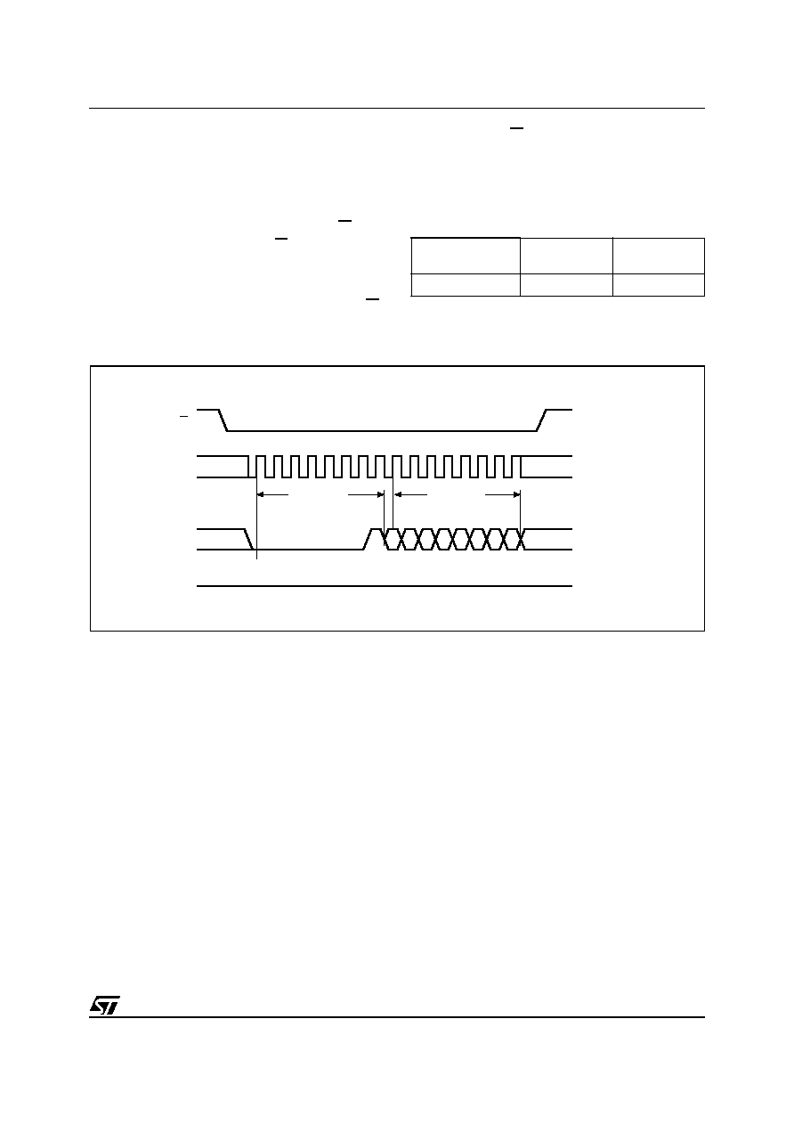
Figure 15. AC Measurement I/O Waveform
Table 15. Capacitance
Note: Sampled only, not 100% tested, at T
A
=25°C and a frequency of 5MHz.
Table 16. DC Characteristics (M95320 and M95640, Device Grade 6)
Note: 1. For all 5V range devices, the device meets the output requirements for both TTL and CMOS standards.
2. Previous product version is identified by Process Identification letter `S'.
3. Current product version is identified by Process Identification letter `V''.
4. New product version is identified by Process Identification letter `P'.
5. Preliminary data.
Symbol
Parameter
Test Condition
Min
.
Max
.
Unit
C
OUT
Output Capacitance (Q)
V
OUT
= 0V
8
pF
C
IN
Input Capacitance (D)
V
IN
= 0V
8
pF
Input Capacitance (other pins)
V
IN
= 0V
6
pF
Symbol
Parameter
Test Condition
Min.
Max.
Unit
I
LI
Input Leakage Current
V
IN
= V
SS
or
V
CC
± 2
µA
I
LO
Output Leakage Current
S = V
CC
, V
OUT
= V
SS
or
V
CC
± 2
µA
I
CC
Supply Current
C = 0.1V
CC
/0.9V
CC
at 5MHz,
V
CC
= 5V, Q = open,
Previous Product
2
4
mA
C = 0.1V
CC
/0.9V
CC
at 10MHz,
V
CC
= 5V, Q = open, Current Product
3
5
mA
C = 0.1V
CC
/0.9V
CC
at 20MHz,
V
CC
= 5V, Q = open, New Product
4,5
10
mA
I
CC1
Supply Current
(Standby)
S = V
CC
, V
CC
= 5V,
V
IN
= V
SS
or
V
CC
, Previous Product
2
10
µA
S = V
CC
, V
CC
= 5V,
V
IN
= V
SS
or
V
CC
, Current Product
3
2
µA
S = V
CC
, V
CC
= 5V,
V
IN
= V
SS
or
V
CC
, New Product
4,5
2
µA
V
IL
Input Low Voltage
0.45
0.3 V
CC
V
V
IH
Input High Voltage
0.7 V
CC
V
CC
+1
V
V
OL
1
Output Low Voltage
I
OL
= 2 mA, V
CC
= 5V
0.4
V
V
OH
1
Output High Voltage
I
OH
= 2 mA, V
CC
= 5V
0.8 V
CC
V
AI00825B
0.8VCC
0.2VCC
0.7VCC
0.3VCC
Input and Output
Timing Reference Levels
Input Levels
25/42
M95640, M95320
Table 17. DC Characteristics (M95320 and M95640, Device Grade 3)
Note: 1. For all 5V range devices, the device meets the output requirements for both TTL and CMOS standards.
2. Previous product version is identified by Process Identification letter `S'.
3. Current product version is identified by Process Identification letters `B'.
4. New product version is identified by Process Identification letters `P'.
5. Preliminary data.
Symbol
Parameter
Test Condition
Min.
Max.
Unit
I
LI
Input Leakage Current
V
IN
= V
SS
or
V
CC
± 2
µA
I
LO
Output Leakage Current
S = V
CC
, V
OUT
= V
SS
or
V
CC
± 2
µA
I
CC
Supply Current
C = 0.1V
CC
/0.9V
CC
at 2MHz,
V
CC
= 5V, Q = open, Previous Product
2
2
mA
C = 0.1V
CC
/0.9V
CC
at 5MHz,
V
CC
= 5V, Q = open, Current Product
3
4
mA
C = 0.1V
CC
/0.9V
CC
at 20MHz,
V
CC
= 5V, Q = open, New Product
4,5
12
mA
I
CC1
Supply Current
(Standby)
S = V
CC
, V
CC
= 5V,
V
IN
= V
SS
or
V
CC
, Previous Product
2
20
µA
S = V
CC
, V
CC
= 5V,
V
IN
= V
SS
or
V
CC
, Current Product
3
5
µA
S = V
CC
, V
CC
= 5V,
V
IN
= V
SS
or
V
CC
, New Product
4,5
2
µA
V
IL
Input Low Voltage
0.45
0.3 V
CC
V
V
IH
Input High Voltage
0.7 V
CC
V
CC
+1
V
V
OL
1
Output Low Voltage
I
OL
= 2mA, V
CC
= 5V
0.4
V
V
OH
1
Output High Voltage
I
OH
= 2mA, V
CC
= 5V
0.8 V
CC
V
M95640, M95320
26/42
Table 18. DC Characteristics (M95320-W and M95640-W, Device Grade 6)
Note: 1. Previous product version is identified by Process Identification letter `S'.
2. Current product version is identified by Process Identification letter `V''.
3. New product version is identified by Process Identification letter `P'.
4. Preliminary data.
Table 19. DC Characteristics (M95320-W and M95640-W, Device Grade 3)
Note: 1. Current product version is identified by Process Identification letter `B'.
2. New product version is identified by Process Identification letter `P'.
Symbol
Parameter
Test Condition
Min.
Max.
Unit
I
LI
Input Leakage Current
V
IN
= V
SS
or
V
CC
± 2
µA
I
LO
Output Leakage Current
S = V
CC
, V
OUT
= V
SS
or
V
CC
± 2
µA
I
CC
Supply Current
C = 0.1V
CC
/0.9V
CC
at 2MHz,
V
CC
= 2.5V, Q = open, Previous Product
1
2
mA
C = 0.1V
CC
/0.9V
CC
at 5MHz,
V
CC
= 2.5V, Q = open, Current Product
2
3
mA
C = 0.1V
CC
/0.9V
CC
at
10MHz,
V
CC
= 2.5V, Q = open, New Product
3,4
5
mA
I
CC1
Supply Current
(Standby)
S = V
CC
, V
CC
= 2.5V,
V
IN
= V
SS
or
V
CC
, Previous Product
1
2
µA
S = V
CC
, V
CC
= 2.5V
V
IN
= V
SS
or
V
CC
, Current Product
2
1
µA
S = V
CC
, V
CC
= 2.5V
V
IN
= V
SS
or
V
CC
, New Product
3,4
1
µA
V
IL
Input Low Voltage
0.45
0.3 V
CC
V
V
IH
Input High Voltage
0.7 V
CC
V
CC
+1
V
V
OL
Output Low Voltage
I
OL
= 1.5mA, V
CC
= 2.5V
0.4
V
V
OH
Output High Voltage
I
OH
= 0.4mA, V
CC
= 2.5V
0.8 V
CC
V
Symbol
Parameter
Test Condition
Min.
Max.
Unit
I
LI
Input Leakage Current
V
IN
= V
SS
or
V
CC
± 2
µA
I
LO
Output Leakage Current
S = V
CC
, V
OUT
= V
SS
or
V
CC
± 2
µA
I
CC
Supply Current
C = 0.1V
CC
/0.9V
CC
at 5MHz,
V
CC
= 2.5V, Q = open, Current Product
1
3
mA
C = 0.1V
CC
/0.9V
CC
at 10MHz,
V
CC
= 2.5V, Q = open, New Product
2
6
mA
I
CC1
Supply Current (Standby)
S = V
CC
, V
CC
= 2.5V, V
IN
= V
SS
or
V
CC
2
µA
V
IL
Input Low Voltage
0.45
0.3 V
CC
V
V
IH
Input High Voltage
0.7 V
CC
V
CC
+1
V
V
OL
Output Low Voltage
I
OL
= 1.5mA, V
CC
= 2.5V
0.4
V
V
OH
Output High Voltage
I
OH
= 0.4mA, V
CC
= 2.5V
0.8 V
CC
V

27/42
M95640, M95320
Table 20. DC Characteristics (M95320-R and M95640-R)
Note: 1. This product is under qualification. For more information, please contact your nearest ST sales office.
2. Preliminary data.
Table 21. DC Characteristics (M95320-S and M95640-S)
Note: 1. This product is under qualification. For more information, please contact your nearest ST sales office.
2. Preliminary data.
Symbol
Parameter
Test Condition
Min.
1,2
Max.
1,2
Unit
I
LI
Input Leakage Current
V
IN
= V
SS
or
V
CC
± 1
µA
I
LO
Output Leakage Current
S = V
CC
, V
OUT
= V
SS
or
V
CC
± 1
µA
I
CC
Supply Current
C = 0.1V
CC
/0.9V
CC
at 5MHz,
V
CC
= 1.8 V, Q = open
3
mA
I
CC1
Supply Current (Standby)
S = V
CC
, V
IN
= V
SS
or
V
CC
, V
CC
= 1.8V
1
µA
V
IL
Input Low Voltage
0.45
0.3 V
CC
V
V
IH
Input High Voltage
0.7 V
CC
V
CC
+1
V
V
OL
Output Low Voltage
I
OL
= 0.15 mA, V
CC
= 1.8 V
0.3
V
V
OH
Output High Voltage
I
OH
= 0.1 mA, V
CC
= 1.8 V
0.8 V
CC
V
Symbol
Parameter
Test Condition
Min.
1,2
Max.
1,2
Unit
I
LI
Input Leakage Current
V
IN
= V
SS
or
V
CC
± 1
µA
I
LO
Output Leakage Current
S = V
CC
, V
OUT
= V
SS
or
V
CC
± 1
µA
I
CC
Supply Current
C = 0.1V
CC
/0.9V
CC
at 2MHz,
V
CC
= 1.65 V, Q = open
1
mA
I
CC1
Supply Current (Standby)
S = V
CC
, V
IN
= V
SS
or
V
CC
, V
CC
= 1.65V
1
µA
V
IL
Input Low Voltage
0.45
0.3 V
CC
V
V
IH
Input High Voltage
0.7 V
CC
V
CC
+1
V
V
OL
Output Low Voltage
I
OL
= 0.15 mA, V
CC
= 1.65V
0.3
V
V
OH
Output High Voltage
I
OH
= 0.1 mA, V
CC
= 1.65V
0.8 V
CC
V
M95640, M95320
28/42
Table 22. AC Characteristics (M95320 and M95640, Device Grade 6)
Note: 1. t
CH
+ t
CL
must never be lower than the shortest possible clock period, 1/f
C
(max).
2. Value guaranteed by characterization, not 100% tested in production.
3. Previous product version is identified by Process Identification letter `S'.
4. Current product version is identified by Process Identification letter `V''.
5. New product version is identified by Process Identification letter `P'.
6. Preliminary Data.
Test conditions specified in
Table 14.
and
Table 10.
Symbol
Alt.
Parameter
Previous
Product
Version
3
Current
Product
Version
4
New Product
Version
5,6
Unit
Min.
Max.
Min.
Max.
Min.
Max.
f
C
f
SCK
Clock Frequency
D.C.
5
D.C.
10
D.C.
20
MHz
t
SLCH
t
CSS1
S Active Setup Time
90
15
15
ns
t
SHCH
t
CSS2
S Not Active Setup Time
90
15
15
ns
t
SHSL
t
CS
S Deselect Time
100
40
20
ns
t
CHSH
t
CSH
S Active Hold Time
90
25
15
ns
t
CHSL
S Not Active Hold Time
90
15
15
ns
t
CH
1
t
CLH
Clock High Time
90
40
20
ns
t
CL
1
t
CLL
Clock Low Time
90
40
20
ns
t
CLCH
2
t
RC
Clock Rise Time
1
1
2
µs
t
CHCL
2
t
FC
Clock Fall Time
1
1
2
µs
t
DVCH
t
DSU
Data In Setup Time
20
15
5
ns
t
CHDX
t
DH
Data In Hold Time
30
15
10
ns
t
HHCH
Clock Low Hold Time after HOLD not Active
70
15
15
ns
t
HLCH
Clock Low Hold Time after HOLD Active
40
20
15
ns
t
CLHL
Clock Low Set-up Time before HOLD Active
0
0
0
ns
t
CLHH
Clock Low Set-up Time before HOLD not
Active
0
0
0
ns
t
SHQZ
2
t
DIS
Output Disable Time
100
25
20
ns
t
CLQV
t
V
Clock Low to Output Valid
60
25
20
ns
t
CLQX
t
HO
Output Hold Time
0
0
0
ns
t
QLQH
2
t
RO
Output Rise Time
50
20
20
ns
t
QHQL
2
t
FO
Output Fall Time
50
20
20
ns
t
HHQV
t
LZ
HOLD High to Output Valid
50
25
20
ns
t
HLQZ
2
t
HZ
HOLD Low to Output High-Z
100
25
20
ns
t
W
t
WC
Write Time
10
5
5
ms
29/42
M95640, M95320
Table 23. AC Characteristics (M95320 and M95640, Device Grade 3)
Note: 1. t
CH
+ t
CL
must never be lower than the shortest possible clock period, 1/f
C
(max).
2. Value guaranteed by characterization, not 100% tested in production.
3. Previous product version is identified by Process Identification letter `S'.
4. Current product version is identified by Process Identification letter `B'.
5. New product version is identified by Process Identification letter `P'.
6. Preliminary Data.
Test conditions specified in
Table 14.
and
Table 10.
Symbol
Alt.
Parameter
Previous
Product
Version
3
Current
Product
Version
4
New
Product
Version
5,6
Unit
Min.
Max.
Min.
Max.
Min.
Max.
f
C
f
SCK
Clock Frequency
D.C.
2
D.C.
5
D.C.
20
MHz
t
SLCH
t
CSS1
S Active Setup Time
200
90
15
ns
t
SHCH
t
CSS2
S Not Active Setup Time
200
90
15
ns
t
SHSL
t
CS
S Deselect Time
200
100
20
ns
t
CHSH
t
CSH
S Active Hold Time
200
90
15
ns
t
CHSL
S Not Active Hold Time
200
90
15
ns
t
CH
1
t
CLH
Clock High Time
200
90
20
ns
t
CL
1
t
CLL
Clock Low Time
200
90
20
ns
t
CLCH
2
t
RC
Clock Rise Time
1
1
2
µs
t
CHCL
2
t
FC
Clock Fall Time
1
1
2
µs
t
DVCH
t
DSU
Data In Setup Time
40
20
5
ns
t
CHDX
t
DH
Data In Hold Time
50
30
10
ns
t
HHCH
Clock Low Hold Time after HOLD not Active
140
70
15
ns
t
HLCH
Clock Low Hold Time after HOLD Active
90
40
15
ns
t
CLHL
Clock Low Set-up Time before HOLD Active
0
0
0
ns
t
CLHH
Clock Low Set-up Time before HOLD not
Active
0
0
0
ns
t
SHQZ
2
t
DIS
Output Disable Time
250
100
20
ns
t
CLQV
t
V
Clock Low to Output Valid
150
60
20
ns
t
CLQX
t
HO
Output Hold Time
0
0
0
ns
t
QLQH
2
t
RO
Output Rise Time
100
50
20
ns
t
QHQL
2
t
FO
Output Fall Time
100
50
20
ns
t
HHQV
t
LZ
HOLD High to Output Valid
100
50
20
ns
t
HLQZ
2
t
HZ
HOLD Low to Output High-Z
250
100
20
ns
t
W
t
WC
Write Time
10
5
5
ms
M95640, M95320
30/42
Table 24. AC Characteristics (M95320-W and M95640-W, Device Grade 6)
Note: 1. t
CH
+ t
CL
must never be lower than the shortest possible clock period, 1/f
C
(max).
2. Value guaranteed by characterization, not 100% tested in production.
3. Previous product version is identified by Process Identification letter `S'.
4. Current product version is identified by Process Identification letter `V''.
5. New product version is identified by Process Identification letter `P'.
6. Preliminary Data.
Test conditions specified in
Table 14.
and
Table 11.
Symbol
Alt.
Parameter
Previous
Product
Version
3
Current
Product
Version
4
New
Product
Version
5,6
Unit
Min.
Max.
Min.
Max.
Min.
Max.
f
C
f
SCK
Clock Frequency
D.C.
2
D.C.
5
D.C.
10
MHz
t
SLCH
t
CSS1
S Active Setup Time
200
90
30
ns
t
SHCH
t
CSS2
S Not Active Setup Time
200
90
30
ns
t
SHSL
t
CS
S Deselect Time
200
100
40
ns
t
CHSH
t
CSH
S Active Hold Time
200
90
30
ns
t
CHSL
S Not Active Hold Time
200
90
30
ns
t
CH
1
t
CLH
Clock High Time
200
90
40
ns
t
CL
1
t
CLL
Clock Low Time
200
90
40
ns
t
CLCH
2
t
RC
Clock Rise Time
1
1
2
µs
t
CHCL
2
t
FC
Clock Fall Time
1
1
2
µs
t
DVCH
t
DSU
Data In Setup Time
40
20
10
ns
t
CHDX
t
DH
Data In Hold Time
50
30
10
ns
t
HHCH
Clock Low Hold Time after HOLD not Active
140
70
30
ns
t
HLCH
Clock Low Hold Time after HOLD Active
90
40
30
ns
t
CLHL
Clock Low Set-up Time before HOLD Active
0
0
0
ns
t
CLHH
Clock Low Set-up Time before HOLD not
Active
0
0
0
ns
t
SHQZ
2
t
DIS
Output Disable Time
250
100
40
ns
t
CLQV
t
V
Clock Low to Output Valid
150
60
40
ns
t
CLQX
t
HO
Output Hold Time
0
0
0
ns
t
QLQH
2
t
RO
Output Rise Time
100
50
40
ns
t
QHQL
2
t
FO
Output Fall Time
100
50
40
ns
t
HHQV
t
LZ
HOLD High to Output Valid
100
50
40
ns
t
HLQZ
2
t
HZ
HOLD Low to Output High-Z
250
100
40
ns
t
W
t
WC
Write Time
10
5
5
ms
31/42
M95640, M95320
Table 25. AC Characteristics (M95320-W and M95640-W, Device Grade 3)
Note: 1. t
CH
+ t
CL
must never be lower than the shortest possible clock period, 1/f
C
(max).
2. Value guaranteed by characterization, not 100% tested in production.
3. Current product version is identified by Process Identification letter `V''.
4. New product version is identified by Process Identification letter `P'.
5. Preliminary Data.
Test conditions specified in
Table 14.
and
Table 11.
Symbol
Alt.
Parameter
Current Product
Version
3
New Product
Version
4,5
Unit
Min.
Max.
Min.
Max.
f
C
f
SCK
Clock Frequency
D.C.
5
D.C.
10
MHz
t
SLCH
t
CSS1
S Active Setup Time
90
30
ns
t
SHCH
t
CSS2
S Not Active Setup Time
90
30
ns
t
SHSL
t
CS
S Deselect Time
100
40
ns
t
CHSH
t
CSH
S Active Hold Time
90
30
ns
t
CHSL
S Not Active Hold Time
90
30
ns
t
CH
1
t
CLH
Clock High Time
90
40
ns
t
CL
1
t
CLL
Clock Low Time
90
40
ns
t
CLCH
2
t
RC
Clock Rise Time
1
2
µs
t
CHCL
2
t
FC
Clock Fall Time
1
2
µs
t
DVCH
t
DSU
Data In Setup Time
20
10
ns
t
CHDX
t
DH
Data In Hold Time
30
10
ns
t
HHCH
Clock Low Hold Time after HOLD not Active
70
30
ns
t
HLCH
Clock Low Hold Time after HOLD Active
40
30
ns
t
CLHL
Clock Low Set-up Time before HOLD Active
0
0
ns
t
CLHH
Clock Low Set-up Time before HOLD not Active
0
0
ns
t
SHQZ
2
t
DIS
Output Disable Time
100
40
ns
t
CLQV
t
V
Clock Low to Output Valid
60
40
ns
t
CLQX
t
HO
Output Hold Time
0
0
ns
t
QLQH
2
t
RO
Output Rise Time
50
40
ns
t
QHQL
2
t
FO
Output Fall Time
50
40
ns
t
HHQV
t
LZ
HOLD High to Output Valid
50
40
ns
t
HLQZ
2
t
HZ
HOLD Low to Output High-Z
100
40
ns
t
W
t
WC
Write Time
5
5
ms

M95640, M95320
32/42
Table 26. AC Characteristics (M95320-R and M95640-R)
Note: 1. t
CH
+ t
CL
must never be lower than the shortest possible clock period, 1/f
C
(max).
2. Value guaranteed by characterization, not 100% tested in production.
3. Preliminary data: this product is under qualification. For more information, please contact your nearest ST sales office.
4. New product version is identified by Process Identification letter `P'.
Test conditions specified in
Table 14.
and
Table 12.
Symbol
Alt.
Parameter
Min.
3,4
Max.
3,4
Unit
f
C
f
SCK
Clock Frequency
D.C.
5
MHz
t
SLCH
t
CSS1
S Active Setup Time
60
ns
t
SHCH
t
CSS2
S Not Active Setup Time
60
ns
t
SHSL
t
CS
S Deselect Time
90
ns
t
CHSH
t
CSH
S Active Hold Time
60
ns
t
CHSL
S Not Active Hold Time
60
ns
t
CH
1
t
CLH
Clock High Time
90
ns
t
CL
1
t
CLL
Clock Low Time
90
ns
t
CLCH
2
t
RC
Clock Rise Time
2
µs
t
CHCL
2
t
FC
Clock Fall Time
2
µs
t
DVCH
t
DSU
Data In Setup Time
20
ns
t
CHDX
t
DH
Data In Hold Time
20
ns
t
HHCH
Clock Low Hold Time after HOLD not Active
60
ns
t
HLCH
Clock Low Hold Time after HOLD Active
60
ns
t
CLHL
Clock Low Set-up Time before HOLD Active
0
0
t
CLHH
Clock Low Set-up Time before HOLD not Active
0
0
t
SHQZ
2
t
DIS
Output Disable Time
80
ns
t
CLQV
t
V
Clock Low to Output Valid
80
ns
t
CLQX
t
HO
Output Hold Time
0
ns
t
QLQH
2
t
RO
Output Rise Time
80
ns
t
QHQL
2
t
FO
Output Fall Time
80
ns
t
HHQV
t
LZ
HOLD High to Output Valid
80
ns
t
HLQZ
2
t
HZ
HOLD Low to Output High-Z
80
ns
t
W
t
WC
Write Time
5
ms
33/42
M95640, M95320
Table 27. AC Characteristics (M95320-S Device Grade 3)
Note: 1. t
CH
+ t
CL
must never be lower than the shortest possible clock period, 1/f
C
(max).
2. Value guaranteed by characterization, not 100% tested in production.
3. Preliminary data: this product is under qualification. For more information, please contact your nearest ST sales office.
4. New product version is identified by Process Identification letter `P'.
Test conditions specified in
Table 14.
and
Table 12.
Symbol
Alt.
Parameter
Min.
3,4
Max.
3,4
Unit
f
C
f
SCK
Clock Frequency
D.C.
2
MHz
t
SLCH
t
CSS1
S Active Setup Time
150
ns
t
SHCH
t
CSS2
S Not Active Setup Time
150
ns
t
SHSL
t
CS
S Deselect Time
200
ns
t
CHSH
t
CSH
S Active Hold Time
150
ns
t
CHSL
S Not Active Hold Time
150
ns
t
CH
1
t
CLH
Clock High Time
200
ns
t
CL
1
t
CLL
Clock Low Time
200
ns
t
CLCH
2
t
RC
Clock Rise Time
2
µs
t
CHCL
2
t
FC
Clock Fall Time
2
µs
t
DVCH
t
DSU
Data In Setup Time
50
ns
t
CHDX
t
DH
Data In Hold Time
50
ns
t
HHCH
Clock Low Hold Time after HOLD not Active
150
ns
t
HLCH
Clock Low Hold Time after HOLD Active
150
ns
t
CLHL
Clock Low Set-up Time before HOLD Active
0
0
t
CLHH
Clock Low Set-up Time before HOLD not Active
0
0
t
SHQZ
2
t
DIS
Output Disable Time
200
ns
t
CLQV
t
V
Clock Low to Output Valid
200
ns
t
CLQX
t
HO
Output Hold Time
0
ns
t
QLQH
2
t
RO
Output Rise Time
200
ns
t
QHQL
2
t
FO
Output Fall Time
200
ns
t
HHQV
t
LZ
HOLD High to Output Valid
200
ns
t
HLQZ
2
t
HZ
HOLD Low to Output High-Z
200
ns
t
W
t
WC
Write Time
10
ms
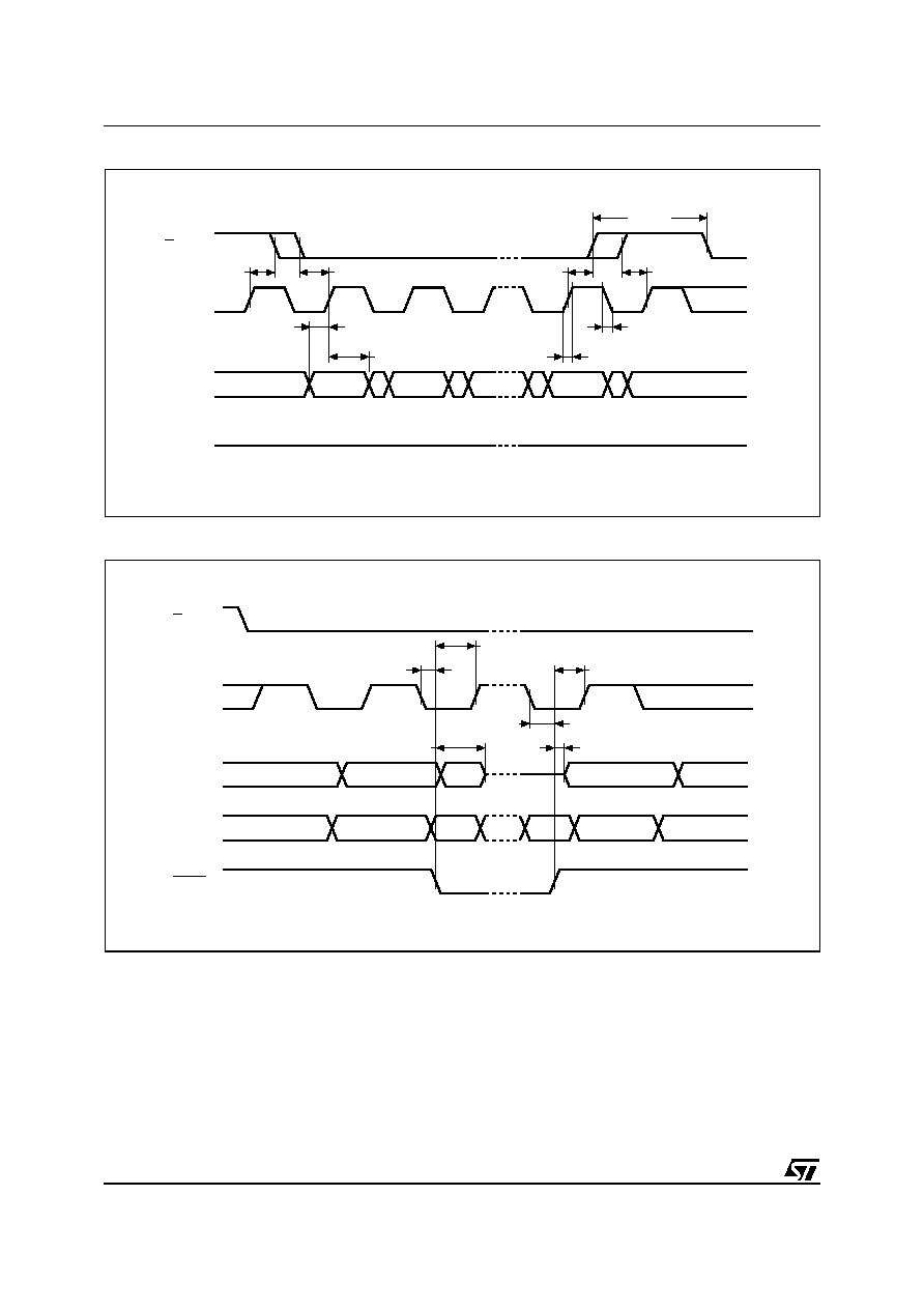
M95640, M95320
34/42
Figure 16. Serial Input Timing
Figure 17. Hold Timing
C
D
AI01447C
S
MSB IN
Q
tDVCH
High Impedance
LSB IN
tSLCH
tCHDX
tCHCL
tCLCH
tSHCH
tSHSL
tCHSH
tCHSL
C
Q
AI01448B
S
D
HOLD
tCLHL
tHLCH
tHHCH
tCLHH
tHHQV
tHLQZ
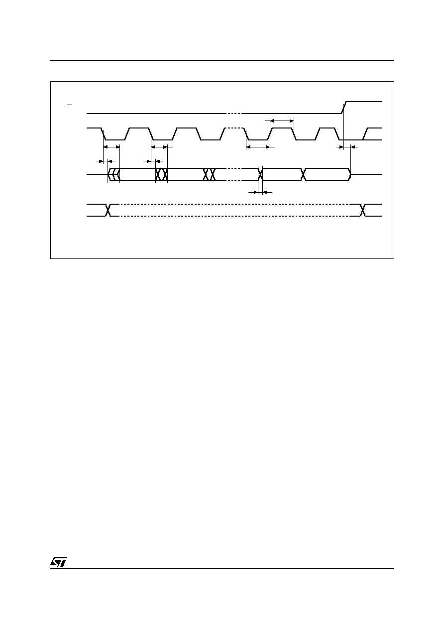
35/42
M95640, M95320
Figure 18. Output Timing
C
Q
AI01449D
S
LSB OUT
D
ADDR.LSB IN
tSHQZ
tCH
tCL
tQLQH
tQHQL
tCLQX
tCLQV
tCLQX
tCLQV
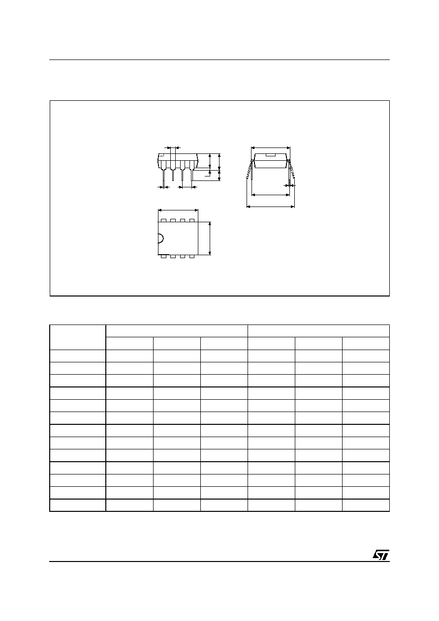
M95640, M95320
36/42
PACKAGE MECHANICAL
Figure 19. PDIP8 8 pin Plastic DIP, 0.25mm lead frame, Package Outline
Note: Drawing is not to scale.
Table 28. PDIP8 8 pin Plastic DIP, 0.25mm lead frame, Package Mechanical Data
Symb.
mm
inches
Typ.
Min.
Max.
Typ.
Min.
Max.
A
5.33
0.210
A1
0.38
0.015
A2
3.30
2.92
4.95
0.130
0.115
0.195
b
0.46
0.36
0.56
0.018
0.014
0.022
b2
1.52
1.14
1.78
0.060
0.045
0.070
c
0.25
0.20
0.36
0.010
0.008
0.014
D
9.27
9.02
10.16
0.365
0.355
0.400
E
7.87
7.62
8.26
0.310
0.300
0.325
E1
6.35
6.10
7.11
0.250
0.240
0.280
e
2.54
0.100
eA
7.62
0.300
eB
10.92
0.430
L
3.30
2.92
3.81
0.130
0.115
0.150
PDIP-B
A2
A1
A
L
b
e
D
E1
8
1
c
eA
b2
eB
E
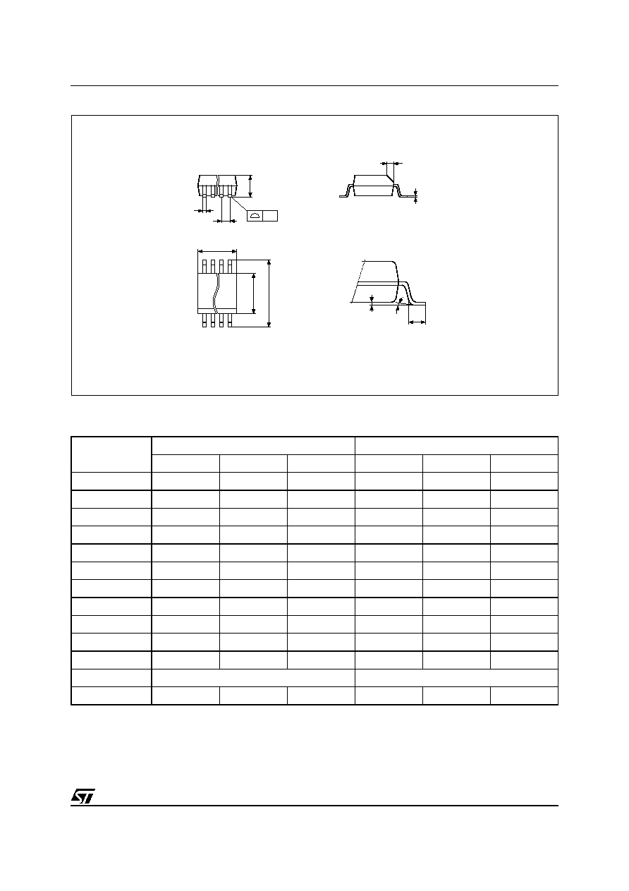
37/42
M95640, M95320
Figure 20. SO8 narrow 8 lead Plastic Small Outline, 150 mils body width, Package Outline
Note: Drawing is not to scale.
Table 29. SO8 narrow 8 lead Plastic Small Outline, 150 mils body width, Package Mechanical Data
Symb.
mm
inches
Typ.
Min.
Max.
Typ.
Min.
Max.
A
1.35
1.75
0.053
0.069
A1
0.10
0.25
0.004
0.010
B
0.33
0.51
0.013
0.020
C
0.19
0.25
0.007
0.010
D
4.80
5.00
0.189
0.197
E
3.80
4.00
0.150
0.157
e
1.27
0.050
H
5.80
6.20
0.228
0.244
h
0.25
0.50
0.010
0.020
L
0.40
0.90
0.016
0.035
0°
8°
0°
8°
N
8
8
CP
0.10
0.004
SO-a
E
N
CP
B
e
A
D
C
L
A1
1
H
h x 45°
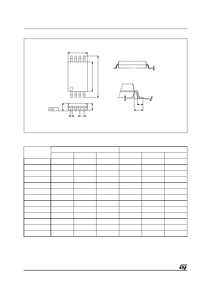
M95640, M95320
38/42
Figure 21. TSSOP8 8 lead Thin Shrink Small Outline, Package Outline
Note: Drawing is not to scale.
Table 30. TSSOP8 8 lead Thin Shrink Small Outline, Package Mechanical Data
Symbol
mm
inches
Typ.
Min.
Max.
Typ.
Min.
Max.
A
1.200
0.0472
A1
0.050
0.150
0.0020
0.0059
A2
1.000
0.800
1.050
0.0394
0.0315
0.0413
b
0.190
0.300
0.0075
0.0118
c
0.090
0.200
0.0035
0.0079
CP
0.100
0.0039
D
3.000
2.900
3.100
0.1181
0.1142
0.1220
e
0.650
0.0256
E
6.400
6.200
6.600
0.2520
0.2441
0.2598
E1
4.400
4.300
4.500
0.1732
0.1693
0.1772
L
0.600
0.450
0.750
0.0236
0.0177
0.0295
L1
1.000
0.0394
0°
8°
0°
8°
TSSOP8AM
1
8
CP
c
L
E
E1
D
A2
A
e
b
4
5
A1
L1
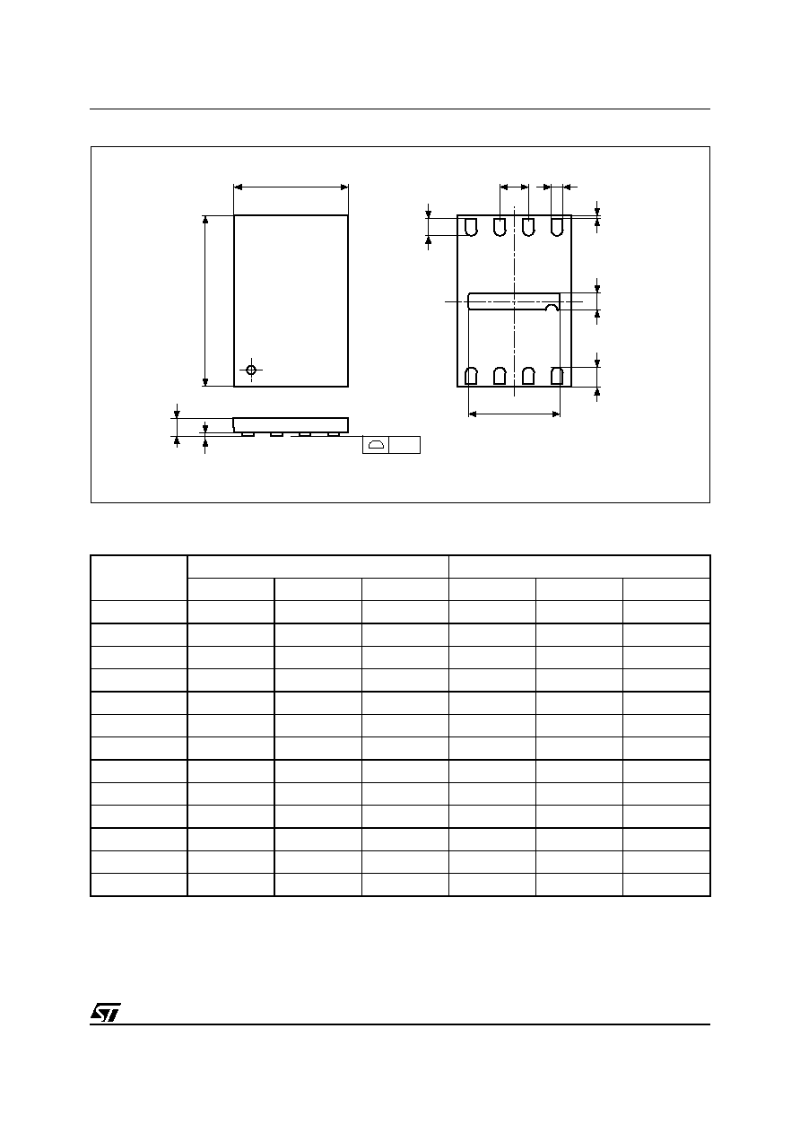
39/42
M95640, M95320
Figure 22. MLP8 - 8-lead Ultra thin Fine pitch Dual Flat No Lead, Package Outline
Note: Drawing is not to scale.
Table 31. MLP8 - 8-lead Ultra thin Fine pitch Dual Flat No Lead, Package Mechanical Data
Symbol
millimeters
inches
Typ
Min
Max
Typ
Min
Max
A
0.55
0.50
0.60
0.022
0.020
0.024
A1
0.00
0.05
0.000
0.002
b
0.25
0.20
0.30
0.010
0.008
0.012
D
2.00
0.079
D2
1.55
1.65
0.061
0.065
ddd
0.05
0.002
E
3.00
0.118
E2
0.15
0.25
0.006
0.010
e
0.50
0.020
L
0.45
0.40
0.50
0.018
0.016
0.020
L1
0.15
0.006
L3
0.30
0.012
N
8
8
D
E
UFDFPN-01
A
A1
ddd
L1
e
b
D2
L
E2
L3
M95640, M95320
40/42
PART NUMBERING
Table 32. Ordering Information Scheme
Note: 1. ST strongly recommends the use of the Automotive Grade devices for use in an automotive environment. The High Reliability Cer-
tified Flow (HRCF) is described in the quality note QNEE9801. Please ask your nearest ST sales office for a copy.
2. Devices bearing the process identification letter "B" or "V" in the package marking (on the top side of the package, on the right side),
guarantee more than 1 million Erase/Write cycle endurance (see
Table 2.
). For more information about these devices, and their
device identification, please contact your nearest ST sales office, and ask for the Product Change Notice.
For a list of available options (speed, package, etc.) or for further information on any aspect of this device,
please contact your nearest ST Sales Office.
Example:
M95640
W MN
6
T
P
Device Type
M95 = SPI serial access EEPROM
Device Function
2
640 = 64 Kbit (8192 x 8)
320 = 32 Kbit (4096 x 8)
Operating Voltage
blank = V
CC
= 4.5 to 5.5V
W = V
CC
= 2.5 to 5.5V
R = V
CC
= 1.8 to 5.5V
S = V
CC
= 1.65 to 5.5V
Package
BN = PDIP8
MN = SO8 (150 mil width)
DW = TSSOP8 (169 mil width)
MB = MLP8 (2x3 mm)
Device Grade
6 = Industrial temperature range, 40 to 85 °C.
Device tested with standard test flow
3 = Device tested with High Reliability Certified Flow
1
.
Automotive temperature range (40 to 125 °C)
Option
blank = Standard Packing
T = Tape and Reel Packing
Plating Technology
blank = Standard SnPb plating
P or G = Lead-Free and RoHS compliant
41/42
M95640, M95320
REVISION HISTORY
Table 33. Document Revision History
Date
Rev.
Description of Revision
13-Jul-2000
1.2
Human Body Model meets JEDEC std (Table 2). Minor adjustments on pp 1,11,15. New clause
on p7. Addition of TSSOP8 package on pp 1, 2, Ordering Info, Mechanical Data
16-Mar-2001
1.3
Test condition added I
LI
and I
LO
, and specification of t
DLDH
and t
DHDL
removed.
t
CLCH
, t
CHCL
, t
DLDH
and t
DHDL
changed to 50ns for the -V range.
"-V" Voltage range changed to "2.7V to 3.6V" throughout.
Maximum lead soldering time and temperature conditions updated.
Instruction sequence illustrations updated.
"Bus Master and Memory Devices on the SPI bus" illustration updated.
Package Mechanical data updated
19-Jul-2001
1.4
M95160 and M95080 devices removed to their own data sheet
06-Dec-2001
1.5
Endurance increased to 1M write/erase cycles
Instruction sequence illustrations updated
18-Dec-2001
2.0
Document reformatted using the new template. No parameters changed.
08-Feb-2002
2.1
Announcement made of planned upgrade to 10MHz clock for the 5V, 40 to 85°C, range.
Endurance set to 100K write/erase cycles
18-Dec-2002
2.2
10MHz, 5MHz, 2MHz clock; 5ms, 10ms Write Time; 100K, 1M erase/write cycles distinguished
on front page, and in the DC and AC Characteristics tables
26-Mar-2003
2.3
Process indentification letter corrected in footnote to AC Characteristics table for temp. range 3
26-Jun-2003
2.4
-S voltage range upgraded by removing it and inserting -R voltage range in its place
15-Oct-2003
3.0
Table of contents, and Pb-free options added. V
IL
(min) improved to -0.45V
21-Nov-2003
3.1
V
I
(min) and V
O
(min) corrected (improved) to -0.45V
28-Jan-2004
4.0
TSSOP8 connections added to DIP and SO connections
24-May-2005
5.0
M95320-S and M95640-S root part numbers (1.65 to 5.5V Supply) and related characteristics
added.
20MHz Clock rate added.TSSOP14 package removed and MLP8 package added.
Description of
Power On Reset: VCC Lock-Out Write Protect
updated.
Product List summary table added. Absolute Maximum Ratings for V
IO
(min) and V
CC
(min)
improved. Soldering temperature information clarified for RoHS compliant devices. Device
Grade 3 clarified, with reference to HRCF and automotive environments. AEC-Q100-002
compliance. t
CHHL
(min) and t
CHHH
(min) is t
CH
for products under "S" process. t
HHQX
corrected
to t
HHQV
.
Figure 17., Hold Timing
updated.

M95640, M95320
42/42
Information furnished is believed to be accurate and reliable. However, STMicroelectronics assumes no responsibility for the consequences
of use of such information nor for any infringement of patents or other rights of third parties which may result from its use. No license is granted
by implication or otherwise under any patent or patent rights of STMicroelectronics. Specifications mentioned in this publication are subject
to change without notice. This publication supersedes and replaces all information previously supplied. STMicroelectronics products are not
authorized for use as critical components in life support devices or systems without express written approval of STMicroelectronics.
The ST logo is a registered trademark of STMicroelectronics.
All other names are the property of their respective owners
© 2005 STMicroelectronics - All rights reserved
STMicroelectronics group of companies
Australia - Belgium - Brazil - Canada - China - Czech Republic - Finland - France - Germany - Hong Kong - India - Israel - Italy - Japan -
Malaysia - Malta - Morocco - Singapore - Spain - Sweden - Switzerland - United Kingdom - United States of America
www.st.com