1/12
July 2001
s
HIGH SPEED:
t
PD
= 27 ns (TYP.) at V
CC
= 6V
s
LOW POWER DISSIPATION:
I
CC
= 4
µ
A(MAX.) at T
A
=25°C
s
HIGH NOISE IMMUNITY:
V
NIH
= V
NIL
= 28 % V
CC
(MIN.)
s
SYMMETRICAL OUTPUT IMPEDANCE:
|I
OH
| = I
OL
= 6mA (MIN)
s
BALANCED PROPAGATION DELAYS:
t
PLH
t
PHL
s
WIDE OPERATING VOLTAGE RANGE:
V
CC
(OPR) = 2V to 6V
s
PIN AND FUNCTION COMPATIBLE WITH
74 SERIES 354
DESCRIPTION
The M74HC354 is an high speed CMOS 8
CHANNEL MULTIPLEXER/REGISTER
(3-STATE) fabricated with silicon gate C
2
MOS
technology.
This device contains an 8 channel digital
multiplexer with an 8-input data register and a
3-bit address input register with 3-state outputs.
The one of eight input data will be provided on the
Y output pin (non-inverted output) and W output
pin (inverted output) determined by the address
data. The information at the data inputs ( D0 to
D7) is stored in the 8-bit latch at the negative pulse
on DC input. The information at the address inputs
(S0 to S2) is stored in the 3-bit latch at the
negative pulse on SC input. These outputs are
disabled to be high-impedance when inputs G1,
G2 are held high or input G3 is held low. This
device is suitable for interfacing with bus lines in a
bus organized system.
The M74HC354 is similar in function to the
M74HC356, which has an 8-bit flip-flop as the data
register instead of an 8-bit latch.
All inputs are equipped with protection circuits
against static discharge and transient excess
voltage.
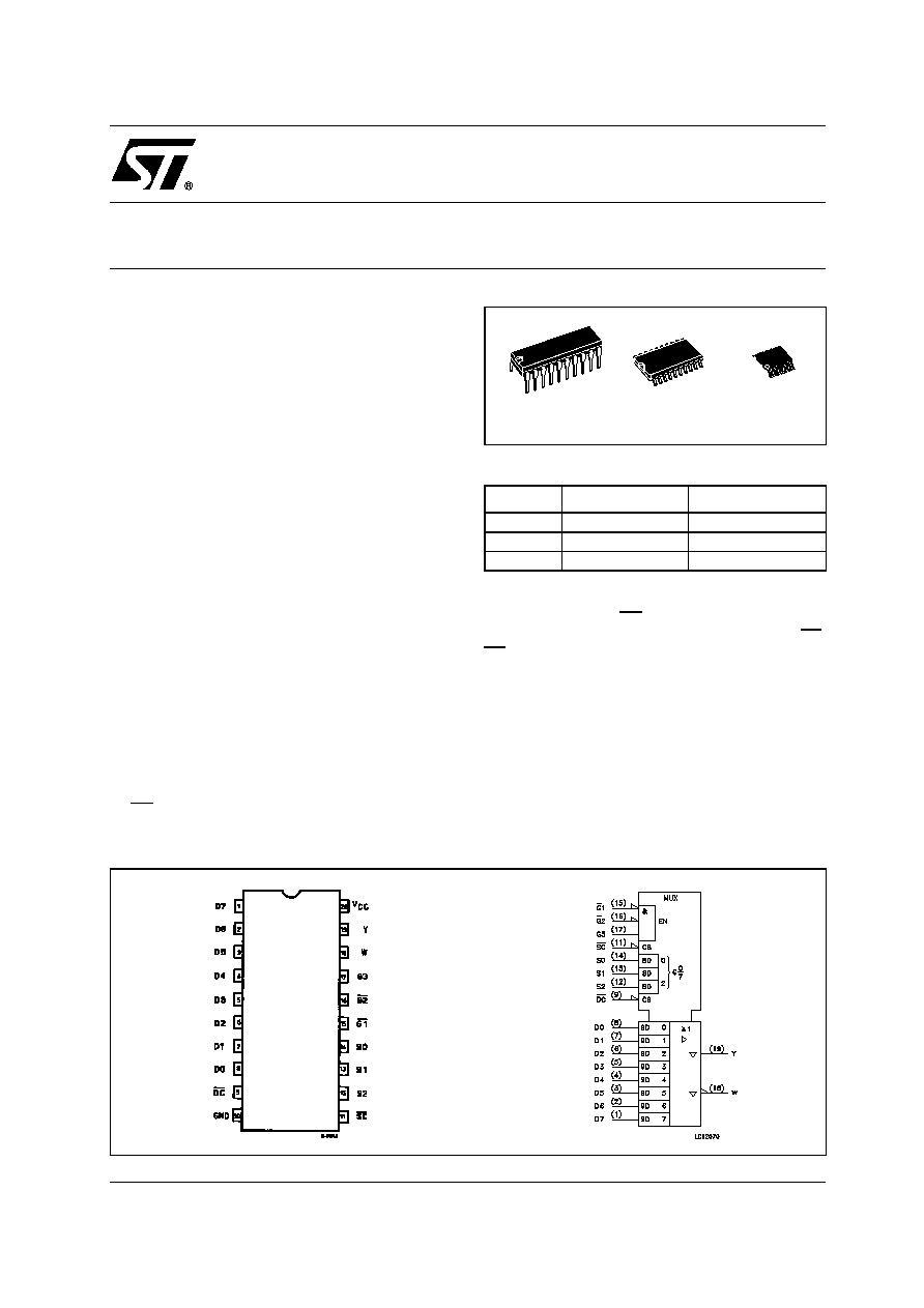
M74HC354
PIN CONNECTION AND IEC LOGIC SYMBOLS
ORDER CODES
PACKAGE
TUBE
T & R
DIP
M74HC354B1R
SOP
M74HC354M1R
M74HC354RM13TR
TSSOP
M74HC354TTR
TSSOP
DIP
SOP
8 CHANNEL MULTIPLEXER/REGISTER (3 STATE)
M74HC354
2/12
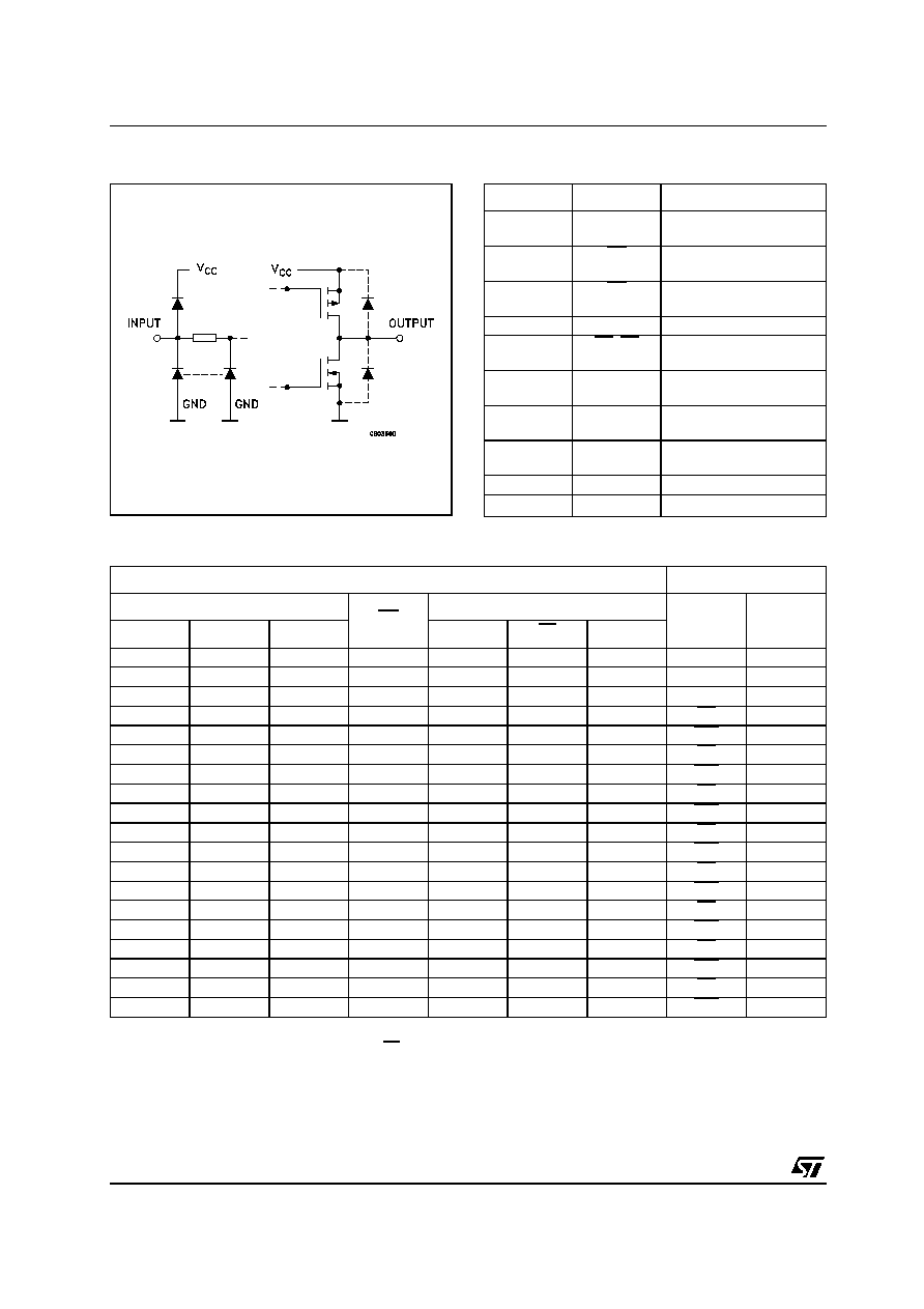
INPUT AND OUTPUT EQUIVALENT CIRCUIT
PIN DESCRIPTION
TRUTH TABLE
X : Don't Care
Z : High Impedance
* : This Column Shows the Input Address Setup with SC low.
D0n....D7n : The level of steady state inputs at input D0 through D7, respectively, before the most recent low to high transition of data control.
PIN No
SYMBOL
NAME AND FUNCTION
8, 7, 6, 5, 4,
3, 2, 1
D0 to D7
Data Inputs
9
DC
Data Enable Input (Active
LOW)
11
SC
Latch Enable Input (Active
LOW)
14, 13, 12
S0, S1, S2
Select Inputs
15, 16
G1, G2
Output Enable Inputs
(Active LOW)
17
G3
Output Enable Input
(Active HIGH)
18
W
3 - state Multiplexer
Output (Active LOW)
19
Y
3 - state Multiplexer
Output (Active HIGH)
10
GND
Ground (0V)
20
V
CC
Positive Supply Voltage
INPUTS
OUTPUTS
SELECT *
DC
OUTPUT ENABLES
W
Y
S2
S1
S0
G1
G2
G3
X
X
X
X
H
X
X
Z
Z
X
X
X
X
X
H
X
Z
Z
X
X
X
X
X
X
L
Z
Z
L
L
L
L
L
L
H
D0
D0
L
L
L
H
L
L
H
D0n
D0n
L
L
H
L
L
L
H
D1
D1
L
L
H
H
L
L
H
D1n
D1n
L
H
L
L
L
L
H
D2
D2
L
H
L
H
L
L
H
D2n
D2n
L
H
H
L
L
L
H
D3
D3
L
H
H
H
L
L
H
D3n
D3n
H
L
L
L
L
L
H
D4
D4
H
L
L
H
L
L
H
D4n
D4n
H
L
H
L
L
L
H
D5
D5
H
L
H
H
L
L
H
D5n
D5n
H
H
L
L
L
L
H
D6
D6
H
H
L
H
L
L
H
D6n
D6n
H
H
H
L
L
L
H
D7
D7
H
H
H
H
L
L
H
D7n
D7n
M74HC354
3/12
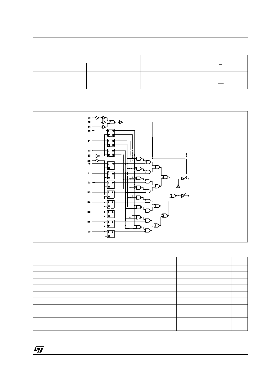
TRUTH TABLE OF INTERNAL LATCH
X : Don't Care
Qn : Data Stored at the trailing edge of the most recent ST pulse.
LOGIC DIAGRAM
ABSOLUTE MAXIMUM RATINGS
Absolute Maximum Ratings are those values beyond which damage to the device may occur. Functional operation under these conditions is
not implied
(*) 500mW at 65
°
C; derate to 300mW by 10mW/
°
C from 65
°
C to 85
°
C
INPUTS
OUTPUTS
D
ST
Q
Q
L
H
L
H
H
H
H
L
X
L
Qn
Qn
Symbol
Parameter
Value
Unit
V
CC
Supply Voltage
-0.5 to +7
V
V
I
DC Input Voltage
-0.5 to V
CC
+ 0.5
V
V
O
DC Output Voltage
-0.5 to V
CC
+ 0.5
V
I
IK
DC Input Diode Current
±
20
mA
I
OK
DC Output Diode Current
±
20
mA
I
O
DC Output Current
±
35
mA
I
CC
or I
GND
DC V
CC
or Ground Current
±
70
mA
P
D
Power Dissipation
500(*)
mW
T
stg
Storage Temperature
-65 to +150
°C
T
L
Lead Temperature (10 sec)
300
°C

M74HC354
4/12
RECOMMENDED OPERATING CONDITIONS
DC SPECIFICATIONS
Symbol
Parameter
Value
Unit
V
CC
Supply Voltage
2 to 6
V
V
I
Input Voltage
0 to V
CC
V
V
O
Output Voltage
0 to V
CC
V
T
op
Operating Temperature
-55 to 125
°C
t
r
, t
f
Input Rise and Fall Time
V
CC
= 2.0V
0 to 1000
ns
V
CC
= 4.5V
0 to 500
ns
V
CC
= 6.0V
0 to 400
ns
Symbol
Parameter
Test Condition
Value
Unit
V
CC
(V)
T
A
= 25°C
-40 to 85°C
-55 to 125°C
Min.
Typ.
Max.
Min.
Max.
Min.
Max.
V
IH
High Level Input
Voltage
2.0
1.5
1.5
1.5
V
4.5
3.15
3.15
3.15
6.0
4.2
4.2
4.2
V
IL
Low Level Input
Voltage
2.0
0.5
0.5
0.5
V
4.5
1.35
1.35
1.35
6.0
1.8
1.8
1.8
V
OH
High Level Output
Voltage
2.0
I
O
=-20
µ
A
1.9
2.0
1.9
1.9
V
4.5
I
O
=-20
µ
A
4.4
4.5
4.4
4.4
6.0
I
O
=-20
µ
A
5.9
6.0
5.9
5.9
4.5
I
O
=-6.0 mA
4.18
4.31
4.13
4.10
6.0
I
O
=-7.8 mA
5.68
5.8
5.63
5.60
V
OL
Low Level Output
Voltage
2.0
I
O
=20
µ
A
0.0
0.1
0.1
0.1
V
4.5
I
O
=20
µ
A
0.0
0.1
0.1
0.1
6.0
I
O
=20
µ
A
0.0
0.1
0.1
0.1
4.5
I
O
=6.0 mA
0.17
0.26
0.33
0.40
6.0
I
O
=7.8 mA
0.18
0.26
0.33
0.40
I
I
Input Leakage
Current
6.0
V
I
= V
CC
or GND
±
0.1
±
1
±
1
µ
A
I
OZ
High Impedance
Output Leakage
Current
6.0
V
I
= V
IH
or V
IL
V
O
= V
CC
or GND
±
0.5
±
5
±
5
µ
A
I
CC
Quiescent Supply
Current
6.0
V
I
= V
CC
or GND
4
40
80
µ
A
M74HC354
5/12
AC ELECTRICAL CHARACTERISTICS (C
L
= 50 pF, Input t
r
= t
f
= 6ns)
Symbol
Parameter
Test Condition
Value
Unit
V
CC
(V)
T
A
= 25°C
-40 to 85°C
-55 to 125°C
Min.
Typ.
Max.
Min.
Max.
Min.
Max.
t
TLH
t
THL
Output Transition
Time
2.0
50
25
60
75
90
ns
4.5
7
12
15
18
6.0
6
10
13
15
t
PLH
t
PHL
Propagation Delay
Time
(Dn, DC - Y, W)
2.0
50
83
210
265
315
ns
4.5
26
42
53
63
6.0
21
36
45
54
2.0
150
99
250
315
375
4.5
31
50
63
75
6.0
25
43
54
64
t
PLH
t
PHL
Propagation Delay
Time (Sn - Y, W)
2.0
50
98
260
325
390
ns
4.5
30
52
65
78
6.0
25
44
55
66
2.0
150
114
300
375
450
4.5
35
60
75
90
6.0
29
51
64
77
t
PLH
t
PHL
Propagation Delay
Time (SC - Y, W)
2.0
50
102
270
340
405
ns
4.5
31
54
68
81
6.0
27
46
58
69
2.0
150
118
310
390
465
4.5
36
62
78
93
6.0
31
53
66
79
t
PZL
t
PZH
High Impedance
Output Enable
Time
2.0
50
R
L
= 1K
44
125
155
190
ns
4.5
14
25
31
38
6.0
12
21
26
32
2.0
150
R
L
= 1K
60
165
205
250
4.5
19
33
41
50
6.0
16
28
35
43
t
PLZ
t
PHZ
High Impedance
Output Disable
Time
2.0
50
R
L
= 1K
42
155
195
235
ns
4.5
20
31
39
47
6.0
17
26
33
40
t
W(L)
Minimum Pulse
Width (DC) (SC)
2.0
50
18
75
95
110
ns
4.5
6
15
19
22
6.0
6
13
16
19
t
S
Minimum Set-up
Time (Dn) (Sn)
2.0
50
10
50
65
75
ns
4.5
3
10
13
15
6.0
3
9
11
13
t
H
Minimum Hold
Time (Dn) (Sn)
2.0
50
5
5
5
ns
4.5
5
5
5
6.0
5
5
5