1/12
March 2000
M68Z512
4 Mbit (512Kb x8) Low Power SRAM with Output Enable
s
ULTRA LOW DATA RETENTION CURRENT
100nA (typical)
10µA (max)
s
OPERATION VOLTAGE: 5V ±10%
s
512 Kbit x8 SRAM with OUTPUT ENABLE
s
EQUAL CYCLE and ACCESS TIMES: 70ns
s
LOW V
CC
DATA RETENTION: 2V
s
TRI-STATE COMMON I/O
s
CMOS for OPTIMUM SPEED/POWER
s
AUTOMATIC POWER-DOWN WHEN
DESELECTED
s
INTENDED FOR USE WITH ST
ZEROPOWER
®
AND TIMEKEEPER
®
CONTROLLERS
DESCRIPTION
The M68Z512 is a 4 Mbit (4,194,304 bit) CMOS
SRAM, organized as 524,288 words by 8 bits. The
device features fully static operation requiring no
external clocks or timing strobes, with equal ad-
dress access and cycle times. It requires a single
5V ±10% supply, and all inputs and outputs are
TTL compatible.
This device has an automatic power-down feature,
reducing the power consumption by over 99%
when deselected.
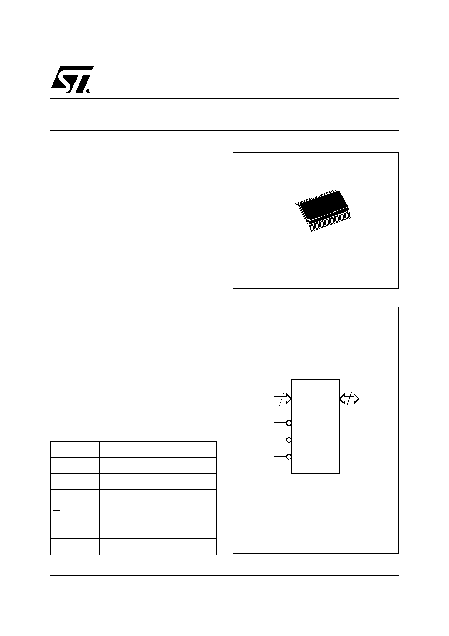
The M68Z512 is available in a 32 lead TSOP II
(10 x 20mm) package.
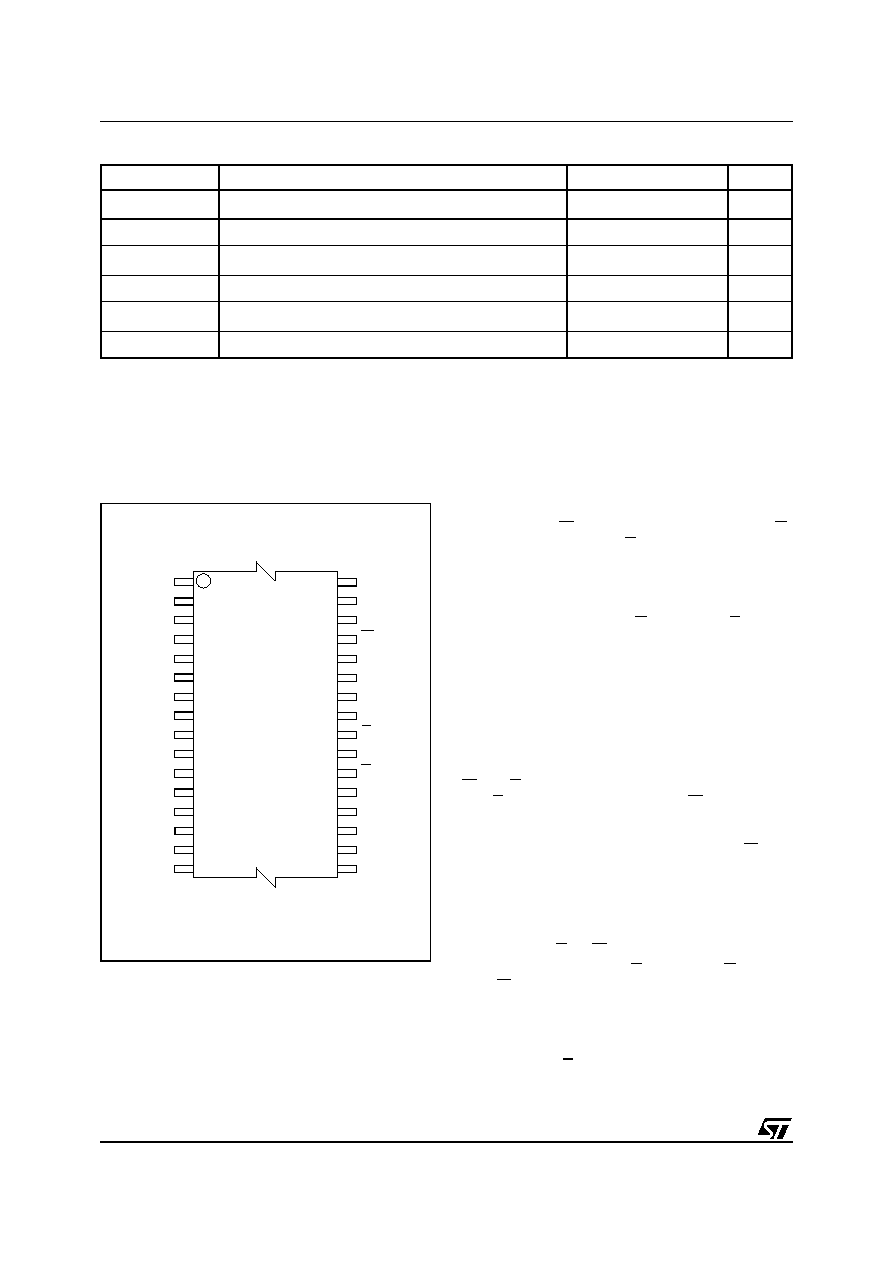
Figure 1. Logic Diagram
AI03030
19
A0-A18
W
DQ0-DQ7
VCC
M68Z512
G
VSS
8
E
32
1
TSOP II 32 (NC)
10 x 20mm
Table 1. Signal Names
A0-A18
Address Inputs
DQ0-DQ7
Data Input/Output
E
Chip Enable
G
Output Enable
W
Write Enable
V
CC
Supply Voltage
V
SS
Ground
M68Z512
2/12
Figure 2. TSOP Connections
DQ5
DQ6
DQ7
DQ0
VSS
DQ3
DQ4
DQ1
DQ2
A12
A15
A14
A16
A6
A17
G
W
A8
A10
A11
A9
A13
A5
A7
A2
A0
A3
A4
A1
AI03031
M68Z512
8
1
9
16
17
24
25
32
VCC
A18
E
Table 2. Absolute Maximum Ratings
(1)
Note: 1. Except for the rating "Operating Temperature Range", stresses above those listed in the Table "Absolute Maximum Ratings" may
cause permanent damage to the device. These are stress ratings only and operation of the device at these or any other conditions
above those indicated in the Operating sections of this specification is not implied. Exposure to Absolute Maximum Rating condi-
tions for extended periods may affect device reliability. Refer also to the STMicroelectronics SURE Program and other relevant qual-
ity documents.
2. Up to a maximum operating V
CC
of 5.5V only.
3. One output at a time, not to exceed 1 second duration.
Symbol
Parameter
Value
Unit
T
A
Ambient Operating Temperature
0 to 70
°C
T
STG
Storage Temperature
65 to 150
°C
V
IO
(2)
Input or Output Voltage
0.3 to V
CC
+ 0.3
V
V
CC
Supply Voltage
0.3 to 7.0
V
I
O
(3)
Output Current
20
mA
P
D
Power Dissipation
1
W
READ MODE
The M68Z512 is in the Read mode whenever
Write Enable (W) is High with Output Enable (G)
Low, and Chip Enable (E) is asserted. This pro-
vides access to data from eight of the 4,194,304
locations in the static memory array, specified by
the 19 address inputs. Valid data will be available
at the eight output pins within t
AVQV
after the last
stable address, providing G is Low and E is Low.
If Chip Enable or Output Enable access times are
not met, data access will be measured from the
limiting parameter (t
ELQV
or t
GLQV
) rather than the
address. Data out may be indeterminate at t
ELQX
and t
GLQX
, but data lines will always be valid at
t
AVQV
.
WRITE MODE
The M68Z512 is in the Write mode whenever the
W and E pins are Low. Either the Chip Enable in-
put (E) or the Write Enable input (W) must be de-
asserted during Address transitions for subse-
quent write cycles. Write begins with the concur-
rence of Chip Enable being active with W low.
Therefore, address setup time is referenced to
Write Enable and Chip Enable as t
AVWL
and t
AVEH
respectively, and is determined by the latter occur-
ring edge.
The Write cycle can be terminated by the earlier
rising edge of E, or W.
if the Output is enabled (E = Low and G = Low),
then W will return the outputs to high impedance
within t
WLQZ
of its falling edge. Care must be taken
to avoid bus contention in this type of operation.
Data input must be valid for t
DVWH
before the ris-
ing edge of Write Enable, or for t
DVEH
before the
rising edge of E, whichever occurs first, and re-
main valid for t
WHDX
or t
EHDX
.
3/12
M68Z512
OPERATIONAL MODE
The M68Z512 has a Chip Enable power down fea-
ture which invokes an automatic standby mode
whenever Chip Enable is de-asserted (E = High).
An Output Enable (G) signal provides a high
speed tri-state control, allowing fast read/write cy-
cles to be achieved with the common I/O data bus.
Operational modes are determined by device con-
trol inputs W and E as summarized in the Operat-
ing Modes table.
Table 3. Operating Modes
Note: 1. X = V
IH
or V
IL
.
Operation
E
W
G
DQ0-DQ7
Power
Read
V
IL
V
IH
V
IH
Hi-Z
Active
Read
V
IL
V
IH
V
IL
Data Output
Active
Write
V
IL
V
IL
X
Data Input
Active
Deselect
V
IH
X
X
Hi-Z
Standby
Table 4. AC Measurement Conditions
Note: Output Hi-Z is defined as the point where data is no longer
driven.
Input Rise and Fall Times
5ns
Input Pulse Voltages
0 to 3V
Input and Output Timing Ref. Voltages
1.5V
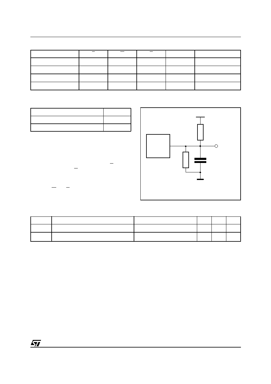
Figure 3. AC Testing Load Circuit
AI03032
5.0V
OUT
CL = 100pF or 5pF
CL includes JIG capacitance
1838
DEVICE
UNDER
TEST
994
Table 5. Capacitance
(1)
(T
A
= 25°C, f = 1 MHz)
Note: 1. Sampled only, not 100% tested.
2. Outputs deselected.
Symbol
Parameter
Test Condition
Min
Max
Unit
C
IN
Input Capacitance on all pins (except DQ)
T
A
= 25°C, f = 1MHz, V
CC
= 5V
6
pF
C
OUT
(2)
Output Capacitance
T
A
= 25°C, f = 1MHz, V
CC
= 5V
8
pF

M68Z512
4/12
Figure 4. Block Diagram
AI03033
ROW
DECODER
A
A
(10)
CHIP ENABLE.
INPUT
DATA
CTRL
DQ
DQ
(8)
COLUMN
DECODER
I/O CIRCUITS
(9)
A
A
CHIP ENABLE.
W
G
MEMORY
ARRAY
VCC
VSS
E
Table 6. DC Characteristics
(T
A
= 0 to 70°C; V
CC
= 5V ±10%)
Note: 1. Average AC current, Outputs open, cycling at t
AVAV
minimum.
2. All other Inputs at V
IL
0.8V or V
IH
2.2V.
3. All other Inputs at V
IL
0.3V or V
IH
V
CC
0.3V.
Symbol
Parameter
Test Condition
Min
Typ
Max
Unit
I
LI
Input Leakage Current
0V
V
IN
V
CC
±1
µA
I
LO
Output Leakage Current
0V
V
OUT
V
CC
±1
µA
I
CC1
(1)
Supply Current
V
CC
= 5.5V, (-55)
90
mA
I
CC2
(2)
Supply Current (Standby) TTL
V
CC
= 5.5V, E = V
IH
15
mA
I
CC3
(3)
Supply Current (Standby) CMOS
V
CC
= 5.5V, E
V
CC
0.3V,
f = 0
1.6
20
µA
V
IL
Input Low Voltage
0.3
0.8
V
V
IH
Input High Voltage
2.2
V
CC
+ 0.3
V
V
OL
Output Low Voltage
I
OL
= 2.1mA
0.4
V
V
OH
Output High Voltage
I
OH
= 1mA
2.4
V

5/12
M68Z512
Figure 5. Address Controlled, Read Mode AC Waveforms
Note: E = Low, G = Low, W = High.
AI03034
tAVAV
tAVQV
tAXQX
A0-A18
DQ0-DQ7
VALID
DATA VALID
Table 7. Read and Standby Modes AC Characteristics
(T
A
= 0 to 70°C; V
CC
= 5V ±10%)
Note: 1. C
L
= 100pF.
2. C
L
= 5pF.
3. At any given temperature and voltage condition, t
EHQZ
is less than t
ELQX
and t
GHQZ
is less than t
GLQX
for any given device.
Symbol
Parameter
M68Z512
Unit
-70
Min
Max
t
AVAV
Read Cycle Time
70
ns
t
AVQV
(1)
Address Valid to Output Valid
70
ns
t
ELQV
(1)
Chip Enable Low to Output Valid
70
ns
t
GLQV
(1)
Output Enable Low to Output Valid
35
ns
t
ELQX
(3)
Chip Enable Low to Output Transition
10
ns
t
GLQX
(3)
Output Enable Low to Output Transition
5
ns
t
EHQZ
(2,3)
Chip Enable High to Output Hi-Z
25
ns
t
GHQZ
(2,3)
Output Enable High to Output Hi-Z
25
ns
t
AXQX
(1)
Address Transition to Output Transition
10
ns
t
PU
Chip Enable Low to Power Up
0
ns
t
PD
Chip Enable High to Power Down
70
ns