M54HC356
M74HC356
January 1993
WITH LATCHES (3-STATE)
8 CHANNEL MULTIPLEXER/REGISTER
B1R
(Plastic Package)
ORDER CODES :
M54HC356F1R
M74HC356M1R
M74HC356B1R
M74HC356C1R
F1R
(Ceramic Package)
M1R
(Micro Package)
C1R
(Chip Carrier)
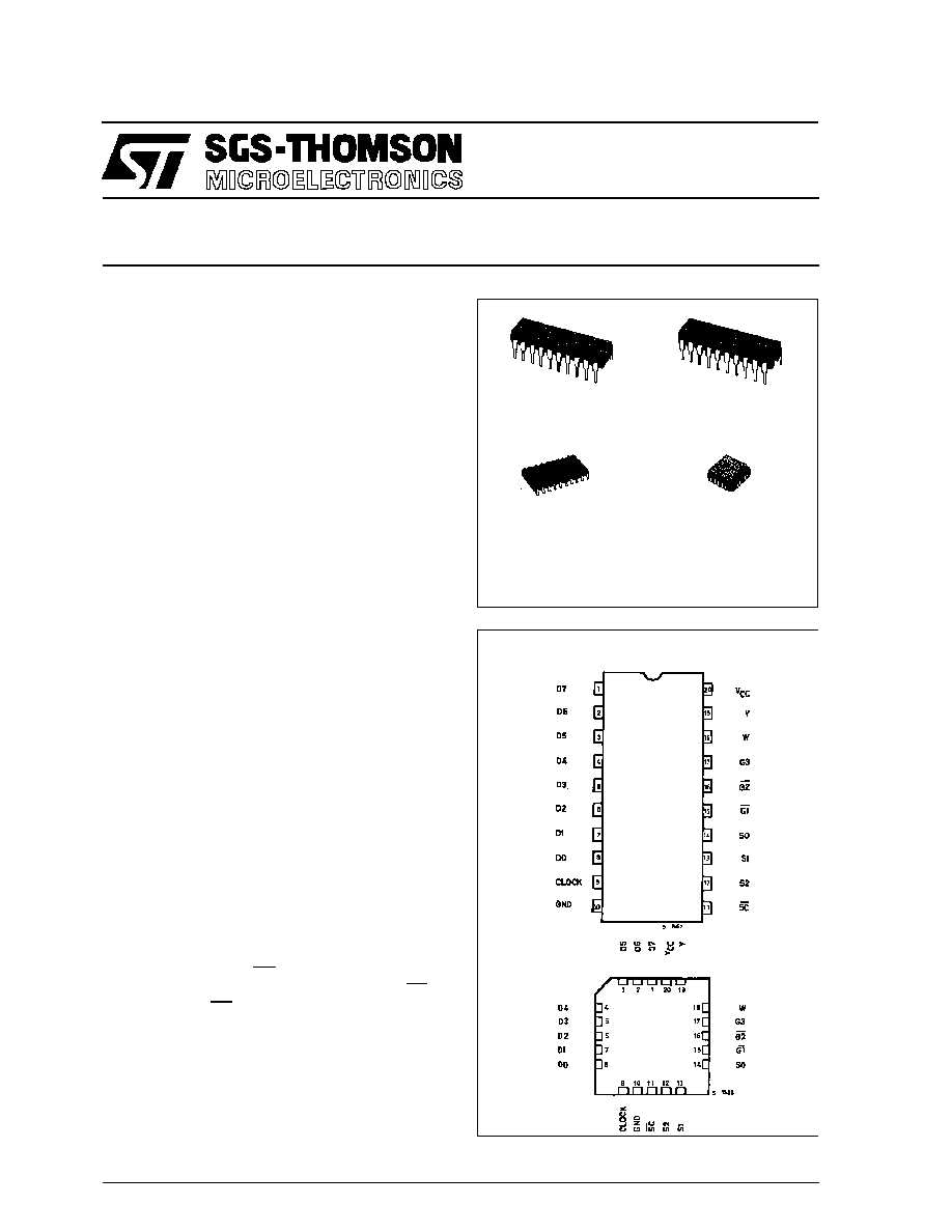
PIN CONNECTIONS (top view)
NC =
No Internal
Connection
DESCRIPTION
.
HIGH SPEED
t
PD
= 25 ns (TYP.) AT V
CC
= 5 V
.
LOW POWER DISSIPATION
I
CC
= 4
�
A (MAX.) AT T
A
= 25
�
C
.
HIGH NOISE IMMUNITY
V
NIH
= V
NIL
= 28 % V
CC
(MIN.)
.
OUTPUT DRIVE CAPABILITY
15 LSTTL LOADS
.
SYMMETRICAL OUTPUT IMPEDANCE
|I
OH
| = I
OL
= 6 mA (MIN.)
.
BALANCED PROPAGATION DELAYS
t
PLH
= t
PHL
.
WIDE OPERATING VOLTAGE RANGE
V
CC
(OPR) = 2 V TO 6 V
.
PIN AND FUNCTION COMPATIBLE WITH
54/74LS356
The M54/74HC356 is a high speed CMOS 8-CHAN-
NEL MULTIPLEXER/REGISTER (3-State) fabri-
cated in silicon gate C
2
MOS technology. It has the
same high speed performance of LSTTL combined
with true CMOS low consumption.
This device contains an 8 channel digital multiplexer
with an 8-bit input data register and a 3-bit address
input register with 3-state outputs. The one of eight
input data will be provided on the Y output pin (non-
inverted output) and W output pin (inverted output)
is determineted by the address data.
The information at the data inputs (D0 to D7) is
stored in the 8-bit flip-flop at the positive going edge
of clock input (CLOCK). The information at the ad-
dress inputs (S0 to S2) is stored in the 3-bit latch at
the negative pulse on SC input. These outputs are
disabled to be high-impedance when input G1 is
held high, input G2 is held high or input G3 is held
low. This device is suitable for interfacing with bus
lines in a bus organized system. The M54/74HC356
is similar in function to the M54/74HC354, which has
an 8-bit latch as the data register instead of an 8-bit
flip-flop. All inputs are equipped with protection cir-
cuits against static discharge and transient excess
voltage.
1/12
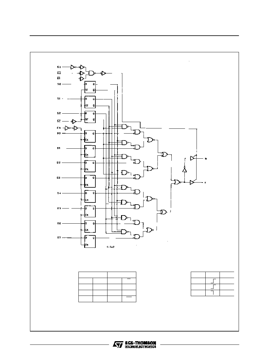
LOGIC DIAGRAM
INPUTS
OUTPUTS
D
ST
Q
Q
L
H
L
H
H
H
H
L
X
L
Qn
Qn
X: DON'T CARE
Qn: DATA STORED AT THE TRAILING
EDGE OF THE MOST RECENT ST
PULSE
D
CK
Q
L
L
H
H
X
Qn
X: DON'T CARE
Qn: NO CHANGE
TRUTH TABLE OF INTERNAL
LATCH
TRUTH TABLE OF INTERNAL
LATCH (FLIP FLOP)
M54/M74HC356
2/12

TRUTH TABLE
INPUTS
SELECT *
CLOCK
OUTPUT ENABLES
W
Y
S2
S1
S0
G1
G2
G3
X
X
X
X
H
X
X
Z
Z
X
X
X
X
X
H
X
Z
Z
X
X
X
X
X
X
L
Z
Z
L
L
L
L
L
H
D0
D0
L
L
L
L
L
H
D0n
D0n
L
L
H
L
L
H
D1
D1
L
L
H
L
L
H
D1n
D1n
L
H
L
L
L
H
D2
D2
L
H
L
L
L
H
D2n
D2n
L
H
H
L
L
H
D3
D3
L
H
H
L
L
H
D3n
D3n
H
L
L
L
L
H
D4
D4
H
L
L
L
L
H
D4n
D4n
H
L
H
L
L
H
D5
D5
H
L
H
L
L
H
D5n
D5n
H
H
L
L
L
H
D6
D6
H
H
L
L
L
H
D6n
D6n
H
H
H
L
L
H
D7
D7
H
H
H
L
L
H
D7n
D7n
X: DON'T CARE Z: HIGH IMPEDANCE *: This column shows the input adress setup with SC LOW.
D1 ..... D7: The level of steady state inputs at input D1 througth D7, respectively, at the time of the LOW to HIGH transition of the clock.
INPUT AND OUTPUT EQUIVALENT CIRCUIT
M54/M74HC356
3/12

PIN DESCRIPTION
PIN No
SYMBOL
NAME AND FUNCTION
8, 7,, 6, 5,
4, 3, 2, 1
D0 to D7
Data Inputs
9
CLOCK
Clock Input (LOW to
HIGH, Edge-triggered)
11
SC
Latch Enable Input
(Active LOW)
14, 13, 12
S0, S1, S2
Select Inputs
15, 16
G1, G2
Output Enable Inputs
(Active LOW)
17
G3
Output Enable Inputs
(Active HIGH)
18
W
3 State Multiplexer Output
(Active LOW)
19
Y
3 State Multiplexer Output
(Active HIGH)
10
GND
Ground (0V)
20
V
CC
Positive Supply Voltage
IEC LOGIC SYMBOL
ABSOLUTE MAXIMUM RATING
Symbol
Parameter
Value
Unit
V
CC
Supply Voltage
-0.5 to +7
V
V
I
DC Input Voltage
-0.5 to V
CC
+ 0.5
V
V
O
DC Output Voltage
-0.5 to V
CC
+ 0.5
V
I
IK
DC Input Diode Current
�
20
mA
I
OK
DC Output Diode Current
�
20
mA
I
O
DC Output Source Sink Current Per Output Pin
�
35
mA
I
CC
or I
GND
DC V
CC
or Ground Current
�
70
mA
P
D
Power Dissipation
500 (*)
mW
T
stg
Storage Temperature
-65 to +150
o
C
T
L
Lead Temperature (10 sec)
300
o
C
Absolute Maximum Ratings are those values beyond which damage to the device may occur. Functional operation under these condition is not implied.
(*) 500 mW:
65
o
C derate to 300 mW by 10mW/
o
C: 65
o
C to 85
o
C
RECOMMENDED OPERATING CONDITIONS
Symbol
Parameter
Value
Unit
V
CC
Supply Voltage
2 to 6
V
V
I
Input Voltage
0 to V
CC
V
V
O
Output Voltage
0 to V
CC
V
T
op
Operating Temperature: M54HC Series
M74HC Series
-55 to +125
-40 to +85
o
C
o
C
t
r
, t
f
Input Rise and Fall Time
V
CC
= 2 V
0 to 1000
ns
V
CC
= 4.5 V
0 to 500
V
CC
= 6 V
0 to 400
M54/M74HC356
4/12
DC SPECIFICATIONS
Symbol
Parameter
Test Conditions
Value
Unit
V
CC
(V)
T
A
= 25
o
C
54HC and 74HC
-40 to 85
o
C
74HC
-55 to 125
o
C
54HC
Min.
Typ.
Max.
Min.
Max.
Min.
Max.
V
IH
High Level Input
Voltage
2.0
1.5
1.5
1.5
V
4.5
3.15
3.15
3.15
6.0
4.2
4.2
4.2
V
IL
Low Level Input
Voltage
2.0
0.5
0.5
0.5
V
4.5
1.35
1.35
1.35
6.0
1.8
1.8
1.8
V
OH
High Level
Output Voltage
2.0
V
I
=
V
IH
or
V
IL
I
O
=-20
�
A
1.9
2.0
1.9
1.9
V
4.5
4.4
4.5
4.4
4.4
6.0
5.9
6.0
5.9
5.9
4.5
I
O
=-6.0 mA
4.18
4.31
4.13
4.10
6.0
I
O
=-7.8 mA
5.68
5.8
5.63
5.60
V
OL
Low Level Output
Voltage
2.0
V
I
=
V
IH
or
V
IL
I
O
= 20
�
A
0.0
0.1
0.1
0.1
V
4.5
0.0
0.1
0.1
0.1
6.0
0.0
0.1
0.1
0.1
4.5
I
O
= 6.0 mA
0.17
0.26
0.33
0.40
6.0
I
O
= 7.8 mA
0.18
0.26
0.33
0.40
I
I
Input Leakage
Current
6.0
V
I
= V
CC
or GND
�
0.1
�
1
�
1
�
A
I
OZ
3 State Output
Off State Current
6.0
V
I
= V
IH
or V
IL
V
O
= V
CC
or GND
�
0.5
�
5.0
�
10
�
A
I
CC
Quiescent Supply
Current
6.0
V
I
= V
CC
or GND
4
40
80
�
A
AC ELECTRICAL CHARACTERISTICS (C
L
= 50 pF, Input t
r
= t
f
= 6 ns)
Symbol
Parameter
Test Conditions
Value
Unit
V
CC
(V)
C
L
(pF)
T
A
= 25
o
C
54HC and 74HC
-40 to 85
o
C
74HC
-55 to 125
o
C
54HC
Min.
Typ.
Max.
Min.
Max.
Min.
Max.
t
TLH
t
THL
Output Transition
Time
2.0
50
25
60
75
90
ns
4.5
7
12
15
18
6.0
6
10
13
15
t
PLH
t
PHL
Propagation
Delay Time
(CLOCK - Y, W)
2.0
50
99
240
300
360
ns
4.5
28
48
60
72
6.0
22
41
51
61
2.0
150
117
280
350
420
ns
4.5
33
56
70
84
6.0
26
48
60
71
M54/M74HC356
5/12