
LE00AB/C
SERIES
VERY LOW DROP
VOLTAGE REGULATORS WITH INHIBIT
®
April 2003
s
VERY LOW DROPOUT VOLTAGE (0.2V TYP.)
s
VERY LOW QUIESCENT CURRENT
(TYP. 50
µ
A IN OFF MODE, 0.5mA IN ON
MODE, NO LOAD)
s
OUTPUT CURRENT UP TO 100 mA
s
OUTPUT VOLTAGES OF 1.25; 1.5; 2.5; 2.7; 3;
3.3; 3.5; 4; 4.5; 4.7; 5; 5.2; 5.5; 6; 8V
s
INTERNAL CURRENT AND THERMAL LIMIT
s
ONLY 2.2
µ
F FOR STABILITY
s
AVAILABLE IN
±
1% (A) OR
±
2% (C)
SELECTION AT 25
o
C
s
SUPPLY VOLTAGE REJECTION: 80 db (TYP.)
s
TEMPERATURE RANGE: -40 TO 125
o
C
DESCRIPTION
The LE00 regulator series are very Low Drop
regulators available in SO-8 and TO-92 packages
and in a wide range of output voltages.
The very Low Drop voltage (0.2V) and the very
low quiescent current make them particularly
suitable for Low Noise Low Power applications
and specially in battery powered systems.
They are pin to pin compatible with the older
L78L00 series. Furthermore in the 8 pin
configuration (SO-8) they employ a Shutdown
Logic Control (pin 5, TTL compatible). This
means that when the device is used as a local
regulator, it's possible to put in stand by a part of
the board even more decreasing the total power
consumption. In the three terminal configuration
(TO-92) the device is even in ON STATE,
mantaining the same electrical performances. It
needs only 2.2
µ
F capacitor for stability allowing
room and cost saving effect.
SCHEMATIC DIAGRAM
SO-8
TO-92
1/25
ABSOLUTE MAXIMUM RATING
Symbol
Parameter
Value
Unit
V
i
DC Input Voltage
20
V
I
o
Output Current
Internally limited (*)
P
tot
Power Dissipation
Internally limited (*)
T
st g
Storage Temperature Range
- 40 to 150
o
C
T
op
Operating Junction Temperature Range
- 40 to 125
o
C
(*) Our SO-8 package used for Voltage Regulators is modified internally to have pins 2, 3, 6 and 7 electrically commoned to the die attach
flag. This particular frame decreases the total thermal resistance of the package and increases its ability to dissipate power when an
appropriate area of copper on the printed circuit board is available for heatsinking. The external dimensions are the same as for the
standard SO-8
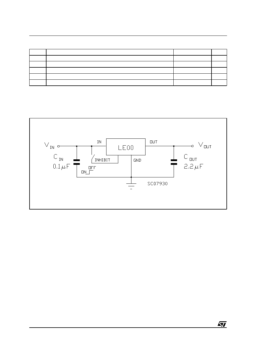
TEST CIRCUITS
Note: If the Inhibit pin is left floating, the regualtor is in ON mode. However, to avoid any noise picking-up, it is suggested to ground it when
the Inhibit function is not used.
LE00AB/C
2/25

CONNECTION DIAGRAM AND ORDERING NUMBERS (top view)
ORDERING NUMBERS
Type
SO-8
TO-92
Output Voltage
LE12AB
LE12C
LE15AB
LE15C
LE25AB
LE25C
LE27AB
LE27C
LE30AB
LE30C
LE33AB
LE33C
LE35AB
LE35C
LE40AB
LE40C
LE45AB
LE45C
LE47AB
LE47C
LE50AB
LE50C
LE52AB
LE52C
LE55AB
LE55C
LE60AB (*)
LE60C (*)
LE80AB (*)
LE80C (*)
LE120AB (*)
LE120C (*)
LE12ABD
LE12CD
LE15ABD
LE15CD
LE25ABD
LE25CD
LE27ABD
LE27CD
LE30ABD
LE30CD
LE33ABD
LE33CD
LE35ABD
LE35CD
LE40ABD
LE40CD
LE45ABD
LE45CD
LE47ABD
LE47CD
LE50ABD
LE50CD
LE52ABD
LE52CD
LE55ABD
LE55CD
LE60ABD
LE60CD
LE80ABD
LE80CD
LE120ABD
LE120CD
LE12ABZ
LE12CZ
LE15ABZ
LE15CZ
LE25ABZ
LE25CZ
LE27ABZ
LE27CZ
LE30ABZ
LE30CZ
LE33ABZ
LE33CZ
LE35ABZ
LE35CZ
LE40ABZ
LE40CZ
LE45ABZ
LE45CZ
LE47ABZ
LE47CZ
LE50ABZ
LE50CZ
LE52ABZ
LE52CZ
LE55ABZ
LE55CZ
LE60ABZ
LE60CZ
LE80ABZ
LE80CZ
LE120ABZ
LE120CZ
1.25 V
1.25 V
1.5 V
1.5 V
2.5 V
2.5 V
2.7 V
2.7 V
3 V
3 V
3.3 V
3.3 V
3.5 V
3.5 V
4 V
4 V
4.5 V
4.5 V
4.7 V
4.7 V
5 V
5 V
5.2 V
5.2 V
5.5 V
5.5 V
6 V
6 V
8 V
8 V
12 V
12 V
(*) Available on request
SO-8
TO-92
pin 1 = OUT
pin 2 = GND
pin 3 = IN
BOTTOM VIEW
LE00AB/C
3/25
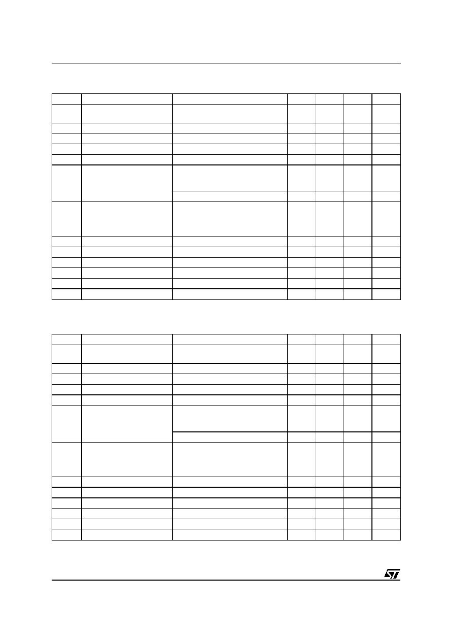
ELECTRICAL CHARACTERISTICS FOR LE12AB (refer to the test circuits, T
j
= 25
o
C,
C
i
= 0.1
µ
F, C
o
= 2.2
µ
F unless otherwise specified)
Symbol
Parameter
Test Conditions
Min.
Typ.
Max.
Unit
V
o
Output Voltage
I
o
= 10 mA, V
i
= 3.3 V
I
o
= 10 mA, V
i
= 3.3 V -25<T
a
<85
o
C
1.225
1.2
1.25
1.275
1.3
V
V
V
i
Operating Input Voltage
I
o
= 100 mA
2.5
18
V
I
out
Output Current Limit
150
mA
V
o
Line Regulation
V
i
= 2.5 to 18 V, I
o
= 0.5 mA
3
15
mV
V
o
Load Regulation
V
i
= 2.8 V I
o
= 0.5 to 100 mA
3
15
mV
I
d
Quiescent Current
ON MODE
V
i
= 2.5 to 18 V I
o
= 0 mA
V
i
= 2.5 to 18 V I
o
= 100 mA
0.5
1.5
1
3
mA
mA
OFF MODE V
i
= 6 V
50
100
µ
A
SVR
Supply Voltage Rejection
I
o
= 5 mA V
i
= 3.5 V
±
1V
f = 120 Hz
f = 1 KHz
f = 10 KHz
82
77
60
dB
dB
dB
eN
Output Noise Voltage
B = 10 Hz to 100 KHz
50
µ
V
V
d
Dropout Voltage
I
o
= 100 mA -40 < T
a
< 125
o
C
1.25
V
V
il
Control Input Logic Low
-40 < T
a
< 125
o
C
0.8
V
V
ih
Control Input Logic High
-40 < T
a
< 125
o
C
2
V
I
i
Control Input Current
V
i
= 6 V, V
c
= 6 V
10
µ
A
C
O
Output Bypass Capacitance
ESR = 0.1 to 10
I
o
= 0 to 100 mA
2
10
µ
F
ELECTRICAL CHARACTERISTICS FOR LE12C (refer to the test circuits, T
j
= 25
o
C,
C
i
= 0.1
µ
F, C
o
= 2.2
µ
F unless otherwise specified)
Symbol
Parameter
Test Conditions
Min.
Typ.
Max.
Unit
V
o
Output Voltage
I
o
= 10 mA, V
i
= 3.3 V
I
o
= 10 mA, V
i
= 3.3 V -25<T
a
<85
o
C
1.225
1.2
1.25
1.275
1.3
V
V
V
i
Operating Input Voltage
I
o
= 100 mA
2.5
18
V
I
out
Output Current Limit
150
mA
V
o
Line Regulation
V
i
= 2.5 to 18 V, I
o
= 0.5 mA
3
20
mV
V
o
Load Regulation
V
i
= 2.8 V I
o
= 0.5 to 100 mA
3
25
mV
I
d
Quiescent Current
ON MODE
V
i
= 2.5 to 18 V I
o
= 0 mA
V
i
= 2.5 to 18 V I
o
= 100 mA
0.5
1.5
1
3
mA
mA
OFF MODE V
i
= 6 V
50
100
µ
A
SVR
Supply Voltage Rejection
I
o
= 5 mA V
i
= 3.5 V
±
1V
f = 120 Hz
f = 1 KHz
f = 10 KHz
82
77
60
dB
dB
dB
eN
Output Noise Voltage
B = 10 Hz to 100 KHz
50
µ
V
V
d
Dropout Voltage
I
o
= 100 mA -40 < T
a
< 125
o
C
1.25
V
V
il
Control Input Logic Low
-40 < T
a
< 125
o
C
0.8
V
V
ih
Control Input Logic High
-40 < T
a
< 125
o
C
2
V
I
i
Control Input Current
V
i
= 6 V, V
c
= 6 V
10
µ
A
C
O
Output Bypass Capacitance
ESR = 0.1 to 10
I
o
= 0 to 100 mA
2
10
µ
F
LE00AB/C
4/25
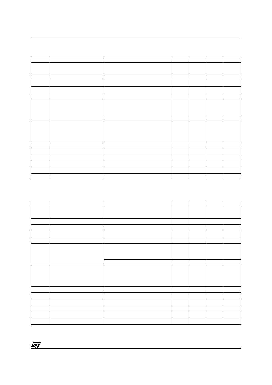
ELECTRICAL CHARACTERISTICS FOR LE15AB (refer to the test circuits, T
j
= 25
o
C,
C
i
= 0.1
µ
F, C
o
= 2.2
µ
F unless otherwise specified)
Symbol
Parameter
Test Conditions
Min.
Typ.
Max.
Unit
V
o
Output Voltage
I
o
= 10 mA, V
i
= 3.5 V
I
o
= 10 mA, V
i
= 3.5 V -25<T
a
<85
o
C
1.47
1.44
1.5
1.53
1.56
V
V
V
i
Operating Input Voltage
I
o
= 100 mA
2.5
18
V
I
out
Output Current Limit
150
mA
V
o
Line Regulation
V
i
= 2.5 to 18 V, I
o
= 0.5 mA
3
15
mV
V
o
Load Regulation
V
i
= 2.8 V I
o
= 0.5 to 100 mA
3
15
mV
I
d
Quiescent Current
ON MODE
V
i
= 2.5 to 18 V I
o
= 0 mA
V
i
= 2.5 to 18 V I
o
= 100 mA
0.5
1.5
1
3
mA
mA
OFF MODE V
i
= 6 V
50
100
µ
A
SVR
Supply Voltage Rejection
I
o
= 5 mA V
i
= 3.5 V
±
1V
f = 120 Hz
f = 1 KHz
f = 10 KHz
82
77
60
dB
dB
dB
eN
Output Noise Voltage
B = 10 Hz to 100 KHz
50
µ
V
V
d
Dropout Voltage
I
o
= 100 mA -40 < T
a
< 125
o
C
1
V
V
il
Control Input Logic Low
-40 < T
a
< 125
o
C
0.8
V
V
ih
Control Input Logic High
-40 < T
a
< 125
o
C
2
V
I
i
Control Input Current
V
i
= 6 V, V
c
= 6 V
10
µ
A
C
O
Output Bypass Capacitance
ESR = 0.1 to 10
I
o
= 0 to 100 mA
2
10
µ
F
ELECTRICAL CHARACTERISTICS FOR LE15C (refer to the test circuits, T
j
= 25
o
C,
C
i
= 0.1
µ
F, C
o
= 2.2
µ
F unless otherwise specified)
Symbol
Parameter
Test Conditions
Min.
Typ.
Max.
Unit
V
o
Output Voltage
I
o
= 10 mA, V
i
= 3.5 V
I
o
= 10 mA, V
i
= 3.5 V -25<T
a
<85
o
C
1.47
1.44
1.5
1.53
1.56
V
V
V
i
Operating Input Voltage
I
o
= 100 mA
2.5
18
V
I
out
Output Current Limit
150
mA
V
o
Line Regulation
V
i
= 2.5 to 18 V, I
o
= 0.5 mA
3
20
mV
V
o
Load Regulation
V
i
= 2.8 V I
o
= 0.5 to 100 mA
3
25
mV
I
d
Quiescent Current
ON MODE
V
i
= 2.5 to 18 V I
o
= 0 mA
V
i
= 2.5 to 18 V I
o
= 100 mA
0.5
1.5
1
3
mA
mA
OFF MODE V
i
= 6 V
50
100
µ
A
SVR
Supply Voltage Rejection
I
o
= 5 mA V
i
= 3.5 V
±
1V
f = 120 Hz
f = 1 KHz
f = 10 KHz
82
77
60
dB
dB
dB
eN
Output Noise Voltage
B = 10 Hz to 100 KHz
50
µ
V
V
d
Dropout Voltage
I
o
= 100 mA -40 < T
a
< 125
o
C
1
V
V
il
Control Input Logic Low
-40 < T
a
< 125
o
C
0.8
V
V
ih
Control Input Logic High
-40 < T
a
< 125
o
C
2
V
I
i
Control Input Current
V
i
= 6 V, V
c
= 6 V
10
µ
A
C
O
Output Bypass Capacitance
ESR = 0.1 to 10
I
o
= 0 to 100 mA
2
10
µ
F
LE00AB/C
5/25