1/12
L9826
October 2002
s
OUTPUTS CURRENT CAPABILITY UP TO
500mA, R
ON
=
2.2
AT T
J
= 25°C
s
PARALLEL CONTROL INPUTS FOR
OUTPUTS 1 AND 2
s
SPI CONTROL FOR OUTPUTS 1 TO 8
s
RESET FUNCTION WITH RESET SIGNAL AT
NRES PIN OR UNDERVOLTAGE AT V
CC
s
- INTRINSIC OUTPUT VOLTAGE CLAMPING
AT TYP. 50V
s
OVERCURRENT SHUTDOWN AT OUTPUTS
3 TO 8
s
SHORT CIRCUIT CURRENT LIMITATION
AND SELECTIVE THERMAL SHUTDOWN AT
OUTPUTS 1 AND 2
s
OUTPUT STATUS DATA AVAILABLE ON THE SPI
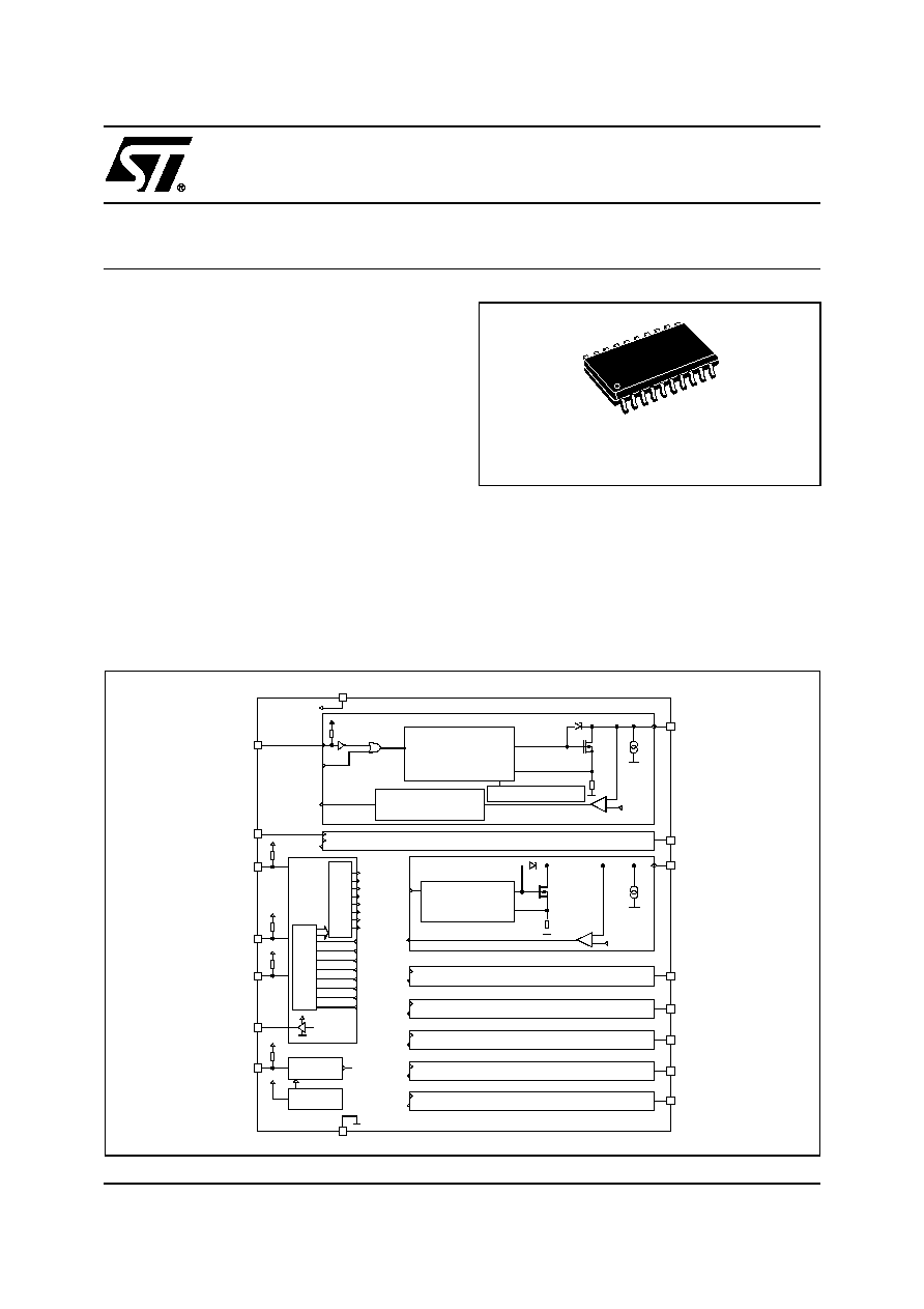
DESCRIPTION
The L9826 is a Octal Low-Side Driver Circuit, dedicated
for automotive applications. Output voltage clamping is
provided for flyback current recirculation, when induc-
tive loads are driven. Chip Select and Serial Peripheral
Interface for outputs control and diagnostic data trans-
fer. Parallel Control inputs for two outputs.
SO20 (16+2+2)
ORDERING NUMBER: L9826
Octal Low-Side Driver for resistive and inductive loads with
serial/parallel input control, output protection and diagnostic
BLOCK DIAGRAM
NCS
SDI
CLK
SDO
NON1
OUT1
OUT2
OUT3
OUT4
OUT5
OUT6
OUT7
OUT8
GND
Diag1
Diag8
nRES
Q1
CH1
Diag1
+
-
CH7
Diag7
Q7
Q1
Q8
CH3
Diag3
Q3
+
-
CH4
CH5
CH6
CH2
NON2
Diag2
Diag4
Q4
Diag5
Q5
Diag6
Q6
Q8
CH8
Diag8
Fault Latch
Q2
Reset
S
h
i
ft R
e
gi
s
t
er
O
u
tpu
t
La
tc
h
SPI
In
t
e
r
f
a
c
e
R
S
Latch / Driver
Reset
Undervoltage
RESET
3
1
2
S
R
Latch / Driver
Q2
Q3
Q4
Q5
Q6
Q7
Diag2
Diag3
Diag4
Diag5
Diag6
Diag7
VCC
VCC
VCC
VCC
VCC
VCC
VCC
VCC
VDG
IOL
IOL
VDG
Overtemperature Detection

L9826
2/12
PIN FUNCTION
PIN CONNECTIONS (Top view)
N°
Pin
Description
1
Out 6
output 6
2
Out 1
output 1
3
nRes
asynchronous nRes
4
NCS
chip select (active low)
5
GND
device ground
6
GND
device ground
7
NON1
control input 1
8
SDO
serial data output
9
Out 8
output 8
10
Out 3
output 3
11
Out 5
output 5
12
Out 2
output 2
13
SDI
serial data input
14
CLK
serial clock
15
GND
device ground
16
GND
device ground
17
NON2
control input 2
18
V
CC
supply voltage
19
Out 7
output 7
20
Out 4
output 4
OUT6
OUT1
nRES
NCS
GND
NON1
GND
SDO
OUT8
OUT2
SDI
CLK
GND
GND
NON2
Vcc
OUT7
OUT4
1
3
2
4
5
6
7
8
9
18
17
16
15
14
12
13
11
19
10
20
OUT3
OUT5
PINCON_L9826

3/12
L9826
ABSOLUTE MAXIMUM RATINGS
For voltages and currents applied externally to the device
Notes: 1. All inputs are protected against ESD according to MIL 883C; tested with HBM at 2KV. It corresponds to a dissipated energy E Ł
0,2mJ.
2. Transient pulses in accordance to DIN40839 part 1, 3 and ISO 7637 Part 1, 3.
For currents determined within the device:
3. When operating the device with short circuit at more than 2 outputs at the same time, damage due to electrical overstress may
occur.
THERMAL DATA
Symbol
Parameter
Test Condition
Min.
Typ.
Max.
Unit
V
CC
Supply voltage
-0.3
7
V
Inputs and data lines
(NONx, NCS, CLK, SDI, nRes)
V
IN
Voltage
(NONx, NCS, CLK, SDI, nRes)
-0.3
7
V
I
IN
Protection diodes current
1)
T
1ms
-20
20
mA
Outputs (Out1 ... Out8)
V
OUTc
Continuous output voltage
-1,0
45
V
I
OUT
Output current
2)
-2
1,0
A
E
OUTcl
Output clamp energy
I
OUT
250mA
10
mJ
Symbol
Parameter
Test Condition
Min.
Typ.
Max.
Unit
Outputs (Out1 ... Out8)
I
OUT
Output current (Out1 ... Out8)
1,0
A
i = 1-8
Total average-current all outputs
3)
2.0
A
Symbol
Parameter
Test Condition
Min.
Typ.
Max.
Unit
Thermal shutdown
T
JSC
Thermal shutdown threshold
150
165
°C
Thermal resistance
R
thjA-one
Single output (junction ambient)
90
°C/W
R
thjA-all
All outputs (junction ambient)
75
°C/W
R
thj-pin
Junction to Pin
18
°C/W
I
O UT i
L9826
4/12
ELECTRICAL CHARACTERISTCS (4.5V
V
CC
5,5V; -40°C
T
J
150°C; unless otherwise specified)
Symbol
Parameter
Test Condition
Min.
Typ.
Max.
Unit
Supply voltage
I
ccSTB
Standby current
without load (nRes = Low)
70
µA
I
ccOPM
Operating mode
I
OUT1 ... 8
= 500mA
SPI - CLK = 3MHz
NCS = LOW
SDO no load
5
mA
I
CC
I
CC
during reverse output
current
I
out
= -2A
100
mA
Inputs (NONx. NCS, CLK, SDI, nRes)
V
INL
Low level
-0.3
0.2·V
CC
V
V
INH
High level
0.7·V
CC
V
CC
+0,3
V
V
hyst
Hysteresis voltage
0.85
V
I
IN
Input current
V
IN
= V
CC
-10
10
µA
R
IN
Pullup resistance
(NONx, NCS, CLK, SDI)
Pulldown resistance (nRes)
50
250
k
C
IN
Input capacitance
10
pF
Serial data outputs
V
SDOH
High output level
I
SDO
= -4mA
V
CC
-0.4
V
V
SDOL
Low output level
I
SDO
= 3,2mA
0.4
V
I
SDOL
Tristate leakage current
NCS = high; 0V
V
SDO
V
CC
-10
10
µA
C
SDO
Output capacitance
f
SDO
= 300kHz
10
pF
Outputs OUT 1 ... 8
I
OUTL1 - 8
Leakage current
OUTx = OFF; V
OUTx
= 25V;
V
CC
= 5V
100
µA
I
OUTL1 - 8
Leakage current
OUTx = OFF; V
OUTx
= 16V;
V
CC
= 5V
100
µA
I
OUTL1 - 8
Leakage current
OUTx = OFF; V
OUTx
= 16V;
V
CC
= 1V
10
µA
V
clp
Output clamp voltage
1mA
I
clp
I
outp
; I
test
= 10mA with
correlation
45
62
V
R
DSon
On resistance OUT 1 ... 8
I
OUT
= 500mA; T
j
= +150°C
3.0
C
OUT
Output capacitance
V
OUT
= 16V; f = 1MHz
300
pF

5/12
L9826
Outputs short circuit protection
I
SBC
Overcurrent shutoff threshold
OUT3 ... OUT8
0.45
1.1
A
I
LIM
Short circuit current limitation
OUT1; OUT2
0.5
1,0
A
t
SCB
Delay shutdown
for output 3 ... 8; I
OUT
1/2 I
SCB
0.2
3,0
12
µs
Diagnostics
V
DG
Diagnostic threshold voltage
0.32·V
CC
0.4·V
C
C
V
I
OL
Open load detection sink
current
V
out
= V
DG
20
100
µA
t
df
Diagnostic detection filter time
for output 1 & 2 on each
diagnostic condition
15
50
µs
Outputs timing
t
don1
Turn ON delay of OUT 1 and 2
NON
1, 2
= 50% to V
OUT
= 0,9·V
bat
NCS = 50% to V
OUT
= 0,9·V
bat
5
µs
t
don2
Turn ON delay of OUT 3 to 8
NCS = 50% to V
OUT
= 0,9·V
bat
10
µs
t
doff
Turn OFF delay of OUT 1 to 8
NCS = 50% to V
OUT
= 0,1·V
bat
NON
1, 2
= 50% to V
OUT
= 0,1·V
bat
10
µs
dU
on1/dt
Turn ON voltage slew-rate
For output 3 to 8; 90% to 30% of
V
bat
; R
L
= 500
; V
bat
= 16V
0.7
3.5
V/µs
dU
on2/dt
Turn ON voltage slew-rate
For output 1 and 2; 90% to 30% of
V
bat
; R
L
= 500
; V
bat
= 16V
2
10
V/µs
dU
off1/dt
Turn OFF voltage slew-rate
For output 1 to 8; 30% to 90% of
V
bat
; R
L
= 500
; V
bat
= 16V
2
10
V/µs
dU
off2/dt
Turn OFF voltage slew-rate
For output 1 to 8; 30% to 80% of
V
bat
; R
L
= 500
; V
bat
= 0.9 · V
clp
2
15
V/µs
Serial diagnostic link (Load capacitor at SDO = 100pF)
f
clk
Clock frequency
50% duty cycle
3
MHz
t
clh
Minimum time CLK = HIGH
160
ns
t
cll
Minimum time CLK = LOW
160
ns
t
pcld
Propagation delay
CLK to data at SDO valid
4,9V
V
CC
5,1V
100
ns
t
csdv
NCS = LOW to data at SDO
active
100
ns
t
sclch
CLK low before NCS low
Setup time CLK to NCS change H/L
100
ns
Symbol
Parameter
Test Condition
Min.
Typ.
Max.
Unit
ELECTRICAL CHARACTERISTCS (continued)

L9826
6/12
FUNCTIONAL DESCRIPTION
General
The L9826 integrated circuit features 8 power low-side-driver outputs. Data is transmitted to the device using
the Serial Peripheral Interface, SPI protocol. Outputs 1 and 2 can be controlled parallel or serial. The power
outputs features voltage clamping function for flyback current recirculation and are protected against short cir-
cuit to Vbat.
The diagnostics recognizes two outputs fault conditions: 1) overcurrent for outputs 3 to 8 , overcurrent and ther-
mal overload for outputs 1 and 2 in switch-on condition and 2) open load or short to GND in switch-off condition
for all outputs. The outputs status can be read out via the serial interface.
The chip internal reset is a OR function of the external nRes signal and internally generated undervoltage nRes
signal.
Output Stages Control
Each output is controlled with its latch and with common reset line, which enables all eight outputs. Outputs 1
and 2 can be controlled also by its NON1, NON2 inputs. It allows PWM control independently on the SPI. These
inputs features internal pull-up resistors to assure that the outputs are switched off, when the inputs are open.
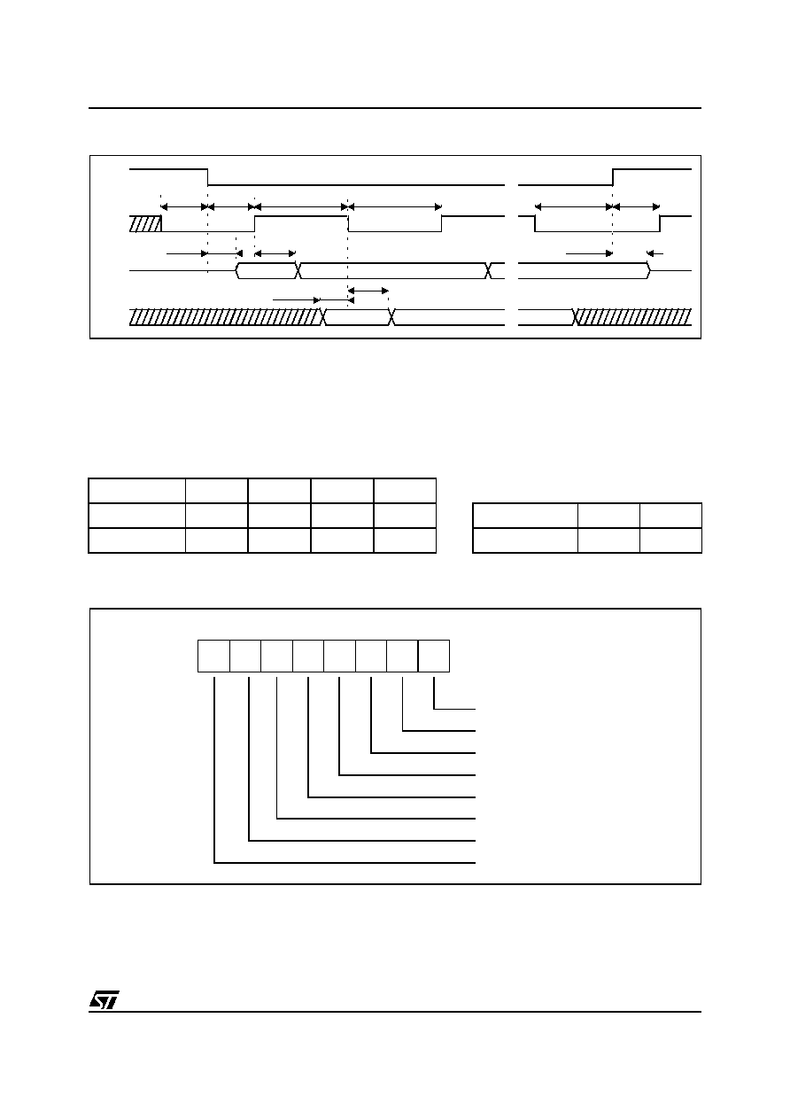
The control data are transmitted via the SDI input, the timing of the serial interface is shown in Fig. 1.
The device is selected with low NCS signal and the input data are transferred into the 8 bit shift register at every
falling CLK edge. The rising edge of the NCS latches the new data from the shift register to the drivers.
t
hclcl
CLK change L/H after NCS =
low
100
ns
t
scld
SDI input setup time
CLK change H/L after SDI data
valid
20
ns
t
hcld
SDI input hold time
SDI data hold after CLK change H/L
20
ns
t
sclcl
CLK low before NCS high
150
ns
t
hclch
CLK high after NCS high
150
ns
t
pchdz
NCS L/H to output data float
100
ns
NCS pulse filter time
Multiple of 8 CLK cycles inside
NCS period
Symbol
Parameter
Test Condition
Min.
Typ.
Max.
Unit
ELECTRICAL CHARACTERISTCS (continued)
7/12
L9826
Figure 1. Timing of the Serial Interface.
The SPI register data are transferred to the output latch at rising NCS edge. The digital filter between NCS and
the output latch ensures that the data are transferred only after 8 CLK cycles or multiple of 8 CLK cycles since
the last NCS falling edge. The NCS changes only at low CLK.
Outputs Control Tables :
Figure 2. Output Control register structure
Outputs 1, 2:
Outputs 3 to 8:
NON1, 2
1
0
0
1
SPI-bit 1, 2
0
0
1
1
SPI-bit 3 ... 8
0
1
Output 1, 2
off
on
on
on
Output 3 ... 8
off
on
NCS
CLK
SDI
SDO
tsclch
thclcl
tclh
tcll
tsclcl
thclch
tcsdv
tpcld
tpchdz
not defined
D8
D1
tscld
thcld
D8
D7
D1
Q2
Q4
Q6
Q8
Q1
Q3
Q5
Q7
MSB
LSB
Control-bit output 7
Control-bit output 5
Control-bit output 3
Control-bit output 1
Control-bit output 8
Control-bit output 6
Control-bit output 4
Control-bit output 2

L9826
8/12
Power outputs characteristics
for flyback current, outputs short circuit protection and diagnostics
For output currents flowing into the circuit the output voltages are limited. The typical value of this voltage is 50V.
This function allows that the flyback current of a inductive load recirculates into the circuit; the flyback energy is
absorbed in the chip.
Output short circuit protection for outputs 3 to 8 (dedicated for loads without inrush current): when the output
current exceeds the short circuit threshold, the corresponding output overload latch is set and the output is
switched off immediately.
Output short circuit protection for outputs 1 and 2 (dedicated for loads with inrush current, as lamps): when the
load current would exceed the short circuit limit value, the corresponding output goes in a current regulation
mode. The output current is determined by the output characteristics and the output voltage depends on the
load resistance. In this mode high power is dissipated in the output transistor and its temperature increases rap-
idly. When the power transistor temperature exceeds the thermal shutdown threshold, the overload latch is set
and the corresponding output switched off.
For the load diagnostic in output off condition each output features a diagnostic current sink, typ 60µA.
Diagnostics
The output voltage at all outputs is compared with the diagnostic threshold, typ 0,38 · V
CC
.
Outputs 1 and 2 features dedicated fault latches. The output status signal is filtered and latched. The fault latch-
es are cleared during NCS low. The latch stores the status bit, so the first reading after the error occurred might
be wrong. The second reading is right.
Diagnostic Table for outputs 1 and 2 in parallel controlled mode:
Fault condition 1) "output short circuit to Vbat" : the output was switched on and the voltage at the output ex-
ceeds the diagnostics threshold. The output operates in current regulation mode or has been switched off due
to thermal shutdown. The status bit is low.
Fault condition 2) "open load" or "output short circuit to GND" : the output is switched off and the voltage at the
output drops below the diagnostics threshold, because the load current is lower than the output diagnostic cur-
rent source, the load is interrupted. The diagnostic bit is low.
For outputs 3 to 8 the output status signals, are fed directly to the SPI register.
Diagnostic Table for outputs 1 to 8 in SPI controlled mode:
Output 1, 2
Output-voltage
Status-bit
Output-mode
off
> DG-threshold
high
correct operation
off
< DG-threshold
low
fault condition 2)
on
< DG-threshold
high
correct operation
on
> DG-threshold
low
fault condition 1)
Output 1 ... 8
Output-voltage
Status-bit
Output-mode
off
> DG-threshold
high
correct operation
off
< DG-threshold
low
fault condition 2)
on
< DG-threshold
low
correct operation
on
> DG-threshold
high
fault condition 1)

9/12
L9826
The fault condition 1) "output short circuit to Vbat" : the output was switched on and the voltage at the output
exceeded the diagnostics threshold due to overcurrent, the output overload latch was set and the output has
been switched off. The diagnostic bit is high.
Fault condition 2) "open load" or "output short circuit to GND" is the same as of outputs 1 and 2.
At the falling edge of NCS the output status data are transferred to the shift register. When NSC is low, data bits
contained in the shift register are transferred to SDO output et every rising CLK edge.
Figure 3. The Pulse Diagram to Read the Outputs Status Register
Figure 4. The Structure of the Outputs Status Register
NCS
CLK
SDI
SDO
MSB
LSB
6
5
4
3
2
1
MSB
LSB
6
5
4
3
2
1
Diag2 Diag4 Diag6 Diag8 Diag1 Diag3 Diag5 Diag7
MSB
LSB
Diagnostic-bit output 7
Diagnostic-bit output 5
Diagnostic-bit output 3
Diagnostic-bit output 1
Diagnostic-bit output 8
Diagnostic-bit output 6
Diagnostic-bit output 4
Diagnostic-bit output 2

L9826
10/12
APPLICATION INFORMATION
The typical application diagram is shown in Fig. 5.
Figure 5. Typical Application Circuit Diagram for the L9826 Circuit.
For higher current driving capability two outputs of the same kind can be paralleled. In this case the maximum
flyback energy should not exceed the limit value for single output.
The immunity of the circuit with respect to the transients at the output is verified during the characterization for
Test Pulses 1, 2 and 3a, 3b, DIN40839 or ISO7637 part 3. The Test Pulses are coupled to the outputs with
200pF series capacitor. All outputs withstand testpulses without damage.
The correct function of the circuit with the Test Pulses coupled to the outputs is verified during the characteriza-
tion for the typical application with R = 30
to 100
, L= 0 to 600mH loads. The Test Pulses are coupled to the
outputs with 200pF series capacitor.
NC
S
2
..
.
7
C
LOC
K
SD
I
SD
O
NRE
S
CC
V
BAT
V
R, L loads
µP
L9826
L9826
VOLTAGE
REGULATOR
NCS
S DI
CLK
SDO
NON1
OUT1
OUT2
OUT3
OUT4
OUT5
OUT6
OUT7
OUT8
GND
Diag1
Diag8
nRES
Q1
CH1
Diag1
+
-
CH7
Diag7
Q7
Q1
Q8
CH3
Diag3
Q3
+
-
CH4
CH5
CH6
CH2
NON2
Diag2
Diag4
Q4
Diag5
Q5
Diag6
Q6
Q8
CH8
Diag8
Fault Latch
Q2
Reset
S
h
if
t
R
e
g
i
st
er
O
u
t
put
La
tc
h
SP
I
In
t
e
r
f
ace
R
S
Latch / Driver
Reset
Undervoltage
RE SET
3
1
2
S
R
Latch / Driver
Q2
Q3
Q4
Q5
Q6
Q7
Diag2
Diag3
Diag4
Diag5
Diag6
Diag7
VCC
VCC
VCC
VCC
VCC
VCC
VCC
VCC
VDG
IOL
IOL
VDG
Overtemperature Detection

11/12
L9826
1
1
0
11
20
A
e
B
D
E
L
K
H
A1
C
SO20MEC
h x 45°
SO20
DIM.
mm
inch
MIN.
TYP.
MAX.
MIN.
TYP.
MAX.
A
2.35
2.65
0.093
0.104
A1
0.1
0.3
0.004
0.012
B
0.33
0.51
0.013
0.020
C
0.23
0.32
0.009
0.013
D
12.6
13
0.496
0.512
E
7.4
7.6
0.291
0.299
e
1.27
0.050
H
10
10.65
0.394
0.419
h
0.25
0.75
0.010
0.030
L
0.4
1.27
0.016
0.050
K
0° (min.)8° (max.)
OUTLINE AND
MECHANICAL DATA

Information furnished is believed to be accurate and reliable. However, STMicroelectronics assumes no responsibility for the consequences
of use of such information nor for any infringement of patents or other rights of third parties which may result from its use. No license is granted
by implication or otherwise under any patent or patent rights of STMicroelectronics. Specifications mentioned in this publication are subject
to change without notice. This publication supersedes and replaces all information previously supplied. STMicroelectronics products are not
authorized for use as critical components in life support devices or systems without express written approval of STMicroelectronics.
The ST logo is a registered trademark of STMicroelectronics
®
2002 STMicroelectronics - All Rights Reserved
STMicroelectronics GROUP OF COMPANIES
Australia - Brazil - Canada - China - Finland - France - Germany - Hong Kong - India - Israel - Italy - Japan -Malaysia - Malta - Morocco -
Singapore - Spain - Sweden - Switzerland - United Kingdom - United States.
http://www.st.com
12/12
L9826