1/12
L9349
September 2002
s
Quad power low side driver with 2 x 5A and
2 x 3A output current capability
s
Low R
DSON
typically 200m
and 300m
@ T
j
= 25°C
s
Internal output clamping structures with
V
FB
= 50V for fast inductive load current
recirculation
s
Limited output voltage slew rate for low EMI
s
Protected
µ
P compatible enable and input
s
Wide operating supply voltage range 4.5V to 32V
s
Real time diagnostic functions:
Output shorted to GND
Output shorted to V
SS
Open load detection in ON and OFF condition
Load bypass detection
Overtemperature detection
s
Device protection functions:
Overload disable
Selective thermal shutdown
s
Signal- and Power-Ground-loss shutdown
DESCRIPTION
The L9349 is a monolithic integrated quad low side
driver realized in an advanced MultipowerBCD mixed
technology. The device is intended to drive valves in
automotive environment.
The inputs are
µ
P compatible. Particular care has
been taken to protect the device against failures, to
avoid electromagnetic interferences and to offer ex-
tensive real time diagnostic.
PowerSO20
BARE DIE
ORDERING NUMBERS:
L9349
L9349DIE1
QUAD INTELLIGENT POWER LOW SIDE SWITCH
BLOCK DIAGRAM
Diagnostic
Control
R
Q
S
Delay
Time
Overload
Overtemp
Output Control
Openload
52V
R
IO
Channel 4
Channel 1
Channel 2
Channel 3
OUT3
OUT2
OUT4
VS
OUT1
IN1
D1
EN
IN4
D4
IN2
D2
IN3
D3
GND
00AT0025

L9349
2/12
PIN CONNECTION
PIN DESCRIPTION
N°
Pin
Function
1
PGND
Power Ground
2
Out1
Output 1 (5A)
3
D1
Diagnostic 1
4
IN4
Input 4
5
VS
Supply Voltage
6
NC
Not Connected
7
IN3
Input 3
8
D2
Diagnostic 2
9
Out2
Output 2 (5A)
10
PGND
Power Ground
11
PGND
Power Ground
12
Out3
Output 3 (3A)
13
D3
Diagnostic 3
14
IN2
Input 2
15
GND
Signal Ground
16
EN
Common Enable
17
IN1
Input 1
18
D4
Diagnostic 4
19
Out4
Output 4 (3A)
20
PGND
Power Ground
20
PGND
19
OUT4
D4
18
IN1
17
16
EN
GND
15
IN2
14
13
D3
OUT3
12
PGND
11
PGND
1
OUT1
2
3
D1
IN4
4
VS
5
6
NC
IN3
7
D2
8
9
OUT2
PGND
10
00AT0026
Heat sink connected
to pins 1, 10, 11, 20
3/12
L9349
THERMAL DATA
ABSOLUTE MAXIMUM RATINGSI
Electrical Characteristcs (Operating Range)
The electrical characteristics are valid within the below defined operating range, unless otherwise specified.
Symbol
Parameter
Value
Unit
R
Th j-case
Thermal resistance junction to case
3
°C/W
Symbol
Parameter
Conditions
Value
Unit
V
S
DC Supply Voltage
-0.3 to 32
V
V
SP
Supply Voltage Pulse (duration <200ms)
-0.3 to 45
V
dV
S
/dt
Supply Voltage Slope
10
V/
µ
s
V
IN, EN
Input Voltage
I
10mA
-1.5 to 6
V
V
D
Diagnostic DC Output Voltage
I
50mA
-0.3 to 16
V
V
ODC
DC Output Voltage
-0.3 to 45
V
I
O1, 2
DC Output Current Out 1, 2
5
A
I
O3, 4
DC Output Current Out 3, 4
3
A
I
OR1, 2
Reverse Output Current
-5
A
I
OR3, 4
Reverse Output Current
-3
A
E
O1, 2
Switch-off Energy for Inductive Loads
t
EO
= 250
µ
s,
1)
1)
t
EO
is the clamping time (see Figure 1)
50
mJ
E
O3, 4
T = 5ms
30
mJ
V
GND
GND Potential Difference
T
j
= -40 to 150°C
±0.3
V
T
jEO
Junction Temperature During Switch-off
t
30 min
175
°C
t
15 min
190
°C
T
j
Junction Temperature
-40 to T
jDIS
°C
T
stg
Storage Temperature
-55 to 150
°C
T
jDIS
Thermal Disable Junction Temp. Threshold
180 to 210
°C
ESD
Electrostatical Discharging
MIL883C
+-2
kV
ESD
OUT1 - 4
vs. Common-GND
(PGNDs + GND)
+-4
kV
Symbol
Parameter
Test Condition
Min.
Typ.
Max.
Unit
V
S
Board Supply Voltage
4.5
12
32
V
T
j1
Junction Temperature
-40
150
°C
T
j2
Junction Temperature
t
15min
1)
over life time
1)
Parameters guaranteed by correlation
150
T
jDIS
°C

L9349
4/12
ELECTRICAL CHARACTERISTICS
(V
S
= 4.5 to 32V; -40°C
T
j1
150°C < T
j2
T
jDIS
, unless other-wise specified.)
Symbol
Parameter
Test Conditions
Values T
j1
Values T
j2
Unit
Min.
Typ.
Max.
Min.
Max.
Supply
I
VS OFF
DC Supply Current Off
EN = 1.0V
5
10
mA
I
VS ON
DC Supply Current On
V
S
14V; V
IN
, V
EN
= 2V
8
mA
Diagnostic Outputs D1 - D4
V
DL
Diagnostic Output Low
Voltage
I
D
3mA
0.65
1.0
1.5
V
I
DLE
Diagnostic Output
Leakage Current
V
D
= 14V
1)
0.1
2
20
µ
A
Outputs Out 1 - Out 4
R
DSON 1, 2
Output On Resistance
T
j
= 25°C
T
j
= 150°C
V
S
> 9.5V I
O1,2
= 2A
200
300
500
m
R
DSON 3, 4
T
j
= 25°C
T
j
= 150°C
V
S
> 9.5V
I
O3,4
= 1.3A
300
450
750
m
V
Z
Z-diode clamping
voltage
I
OCL
200mA
45
60
V
R
O
Output pull down
resistor
VS > 9.5V
EN = 0V
10
40
50
k
V
OUV 1-4
Open Load Voltage
Threshold
V
IN
= 1V
0.525 x
V
S
0.55 x
V
S
0.575 x
V
S
V
V
OUV hys 1-
4
Hysteresis
0.003 x
V
S
V
V
OUV 1-4,
2-3, 4-1, 3-2
Open Load Difference
Voltage Threshold
V
IN1,4/2,3
= 1V V
S
16V
VOc S 4.5V
V
OC
= output voltage of
other channel
V
OC
-
1.0V
V
OC
-
1.25V
V
OC
-
1.5V
V
V
OUV hys
1-4, 2-3,
4-1, 3-2
Open Load Hysteresis
40
mV
I
OUC 1, 2, 3,
4
Open Load Current
Threshold
V
EN
=V
IN
=2V;
V
S
=6.5 - 16V
160
320
480
mA
I
OOC 1, 2
Over Load Current
Threshold
V
S
> 6.5V;
V
OUT
= 32V
5
10
A
I
OOC 3, 4
3
6
A
T
SD
Thermal Shut Down
180
195
210
°C
T
SD-hys
Thermal Shut Down
hysteresis
20
°C
5/12
L9349
I
OUT-LE
OUT leakage current
V
OUT
= 20V
V
S
= 0V
5
µ
A
Inputs IN1-4, EN
V
IN,EN L
Logic Input/Enable
Low Voltage
-0.3
1
V
V
IN,EN H
Logic Input/Enable
High Voltage
IN, EN
2.0
6
V
V
EN,IN hys
Logic Input Hysteresis
50
100
mV
I
IN
Input Sink Current
2V < V
IN
, V
EN
< 6V
2)
V
IN
, V
EN
< V
s
10
20
40
µ
A
I
EN
Enable Sink Current
10
20
40
µ
A
Timing
t
ON
Output Delay ON Time I
O
=
1A
V
S
= 12V
3)
)
Fig. 2
4
25
µ
s
t
f,r
Output fall and rise
time
I
O
=
1A
V
S
= 12V
Fig. 2
3
10
30
µ
s
t
OFF
Output Delay OFF
Time
I
O
=
1A
V
S
= 12V
3)
Fig. 2
5
15
30
µ
s
t
DH-L, Diag
Diag. Delay Output
OFF Time
3)
Fig. 2
8
65
90
µ
s
t
D IOU
Diagnostic Open Load
Delay Time
9V< V
S
<16V, Fig 3
8
50
µ
s
t
DOL
Diagnostic Overload
Delay Switch-OFF
Time
9V< V
S
<16V, Fig 3
6
65
µ
s
t
filt
Filter time
4
24
µ
s
PGND
PGND
loss,h
Power GND loss
threshold high
3
V
PGND
loss,l
Power GND loss
threshold low
2
V
1)
The diagnostic output is short circuit protected up to V
D
= 16V
2)
Open pins (EN, IN) are detected as low
3)
V
S
= 9 to 16V
I
OUC
I
O
I
OOC
ELECTRICAL CHARACTERISTICS (continued)
(V
S
= 4.5 to 32V; -40°C
T
j1
150°C < T
j2
T
jDIS
, unless other-wise specified.)
Symbol
Parameter
Test Conditions
Values T
j1
Values T
j2
Unit
Min.
Typ.
Max.
Min.
Max.
L9349
6/12
DIAGNOSTIC TABLE
CIRCUIT DESCRIPTION
The L9349 is a quad low side driver for inductive loads like valves in automotive environment. The internal pull
down current sources at the ENable and INput pins assure in case of open input conditions that the device is
switched off. An output voltage slope limitation for du/dt is implemented to reduce the EMI. An integrated active
flyback voltage limitation clamps the output voltage during the flyback phase to 50 V.
Each driver is protected against short circuit at V
OUT
< 32V and thermal overload. In short circuit condition the
output will be disabled after a short delay time t
DOL
. The thermal disable for T
J
> 180°C of the output will be
reset if the junction temperature decreases about 20°C below the disable threshold temperature.
The overtemperature, overload and groundloss information is stored until IN is low.
For the real time error diagnosis the voltage and the current of the outputs are compared with internal fixed val-
ues V
OUV
for OFF and I
OUC
for ON conditions to recognize open load (R
L
20K
, R
L
> 38
) in OFF and ON
conditions.
Also the output voltages V
O1- 4
are compared to each other output in OFF condition with a fixed offset of
V
OUV
to recognize load bypasses. The
V
OUV
diagnoses is suppressed during the flyback phases of the compared
output. The outputs 1 and 4 are compared for
V
OUV
and also outputs 2 and 3 are compared.
The diagnostic output level in connection with different ENable and INput conditions allows to recognize differ-
ent fail states, like overtemp, short to V
S
, short to GND, bypass to GND and disconnected load (see diagnostic
table).
The diagnostic output is protected against short circuit. Exceeding the over load current threshold I
OOC
, the out-
put current will be limited internally during the diagnostic overload delay switch-off time t
DOL
.
The device complies the I
SO
pulses imposed to the supply voltage of the valves without any failures of the func-
tionality. Therefore some diagnostic functions are internal filtered. The following table shows the corresponding
filter time for each detected signal.
Conditions
EN
IN
OUT
DIAG.
Normal Function
L
X
off
L
H
L
off
L
H
H
on
H
GND short
V
Otyp
< 0.55VS
L
X
off
H
Load bypass
V
O1-4/2-3
1.25V
H
L
off
H
Open Load
I
O1,2,3,4typ
< 320mA
H
H
on
L
T
jtyp
190°C Overtemperature
X
X
off
L
Over Load
I
Omin 1,2
> 5A
I
Omin 3,4
> 3A
H
H
off
L
SGND or PGND loss
channel off
X
L
off
H
SGND or PGND loss
channel on
H
H
off
L
7/12
L9349
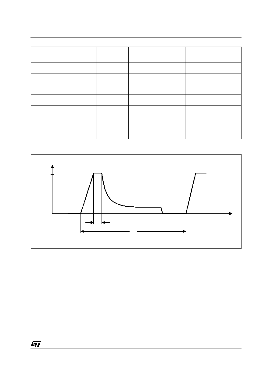
Figure 1. t
EO
Clamping Time
ON State
EN and IN =
HIGH
OFF State
EN or IN,
= LOW
min. Filter
time
Reset done by
Overloading of output
(also shorted load to supply)
X
4
µ
s
INx = "LOW"
Open load
(under voltage detection)
X
-
Open load
(under current detection)
X
-
Overtemperature
X
4
µ
s
INx = "LOW"
Power-Signal GND-loss
X
4
µ
s
INx = "LOW"
Power- Signal-GND-loss
X
4
µ
s
Openload difference
X
4
µ
s
V
O1-4
t
V
OCL
V
S
t
EO
T
00AT0027
L9349
8/12
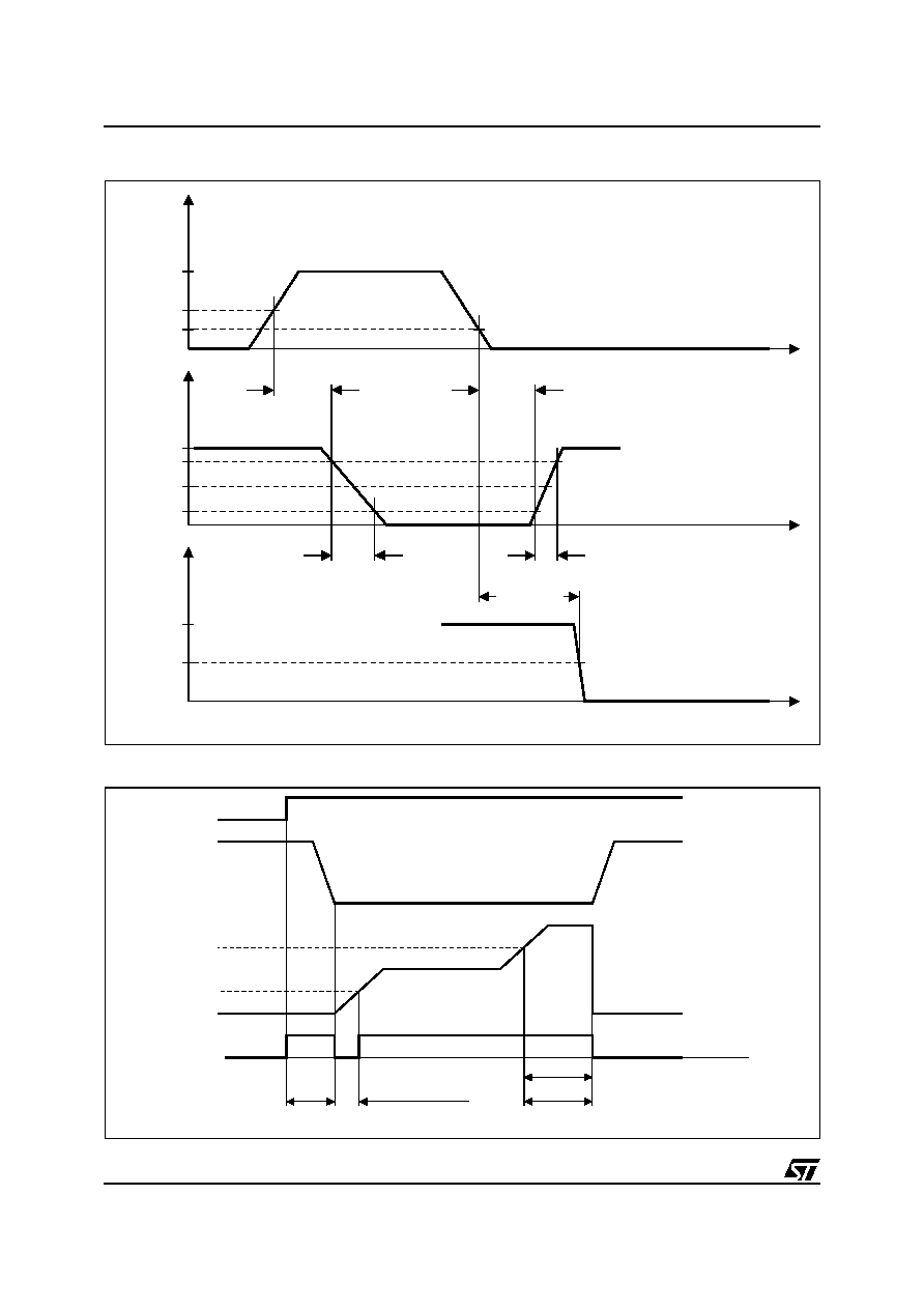
Figure 2. Output Slope (resistive load for testing)
Figure 3. Timing (t
DOL
, t
DIOU
)
V
IN
t
V
H
V
L
5V
V
OUT
t
V
OUV
0.15V
S
t
ON
t
OFF
V
DIAG
0.5V
D
V
D
t
D H-L Diag
00AT0030
V
S
0.85V
S
t
f
t
r
V
EN
IN
V
ON
I
OOC
V
D
I
OUC
Open Load Current
t
DOL
t
DIOU
00AT0032
t
filt

9/12
L9349
Figure 4. Block Diagram - Open Load Voltage Detection
R
IO
R
IO
OUT1
(OUT2)
L
1
(L
2
)
L
4
(L
3
)
V
Batt
OUT4
(OUT3)
+
±
±
+
R
Latch
S
Q
R
Latch
Q
S
V
S
55%
Enable
IN
4
IN
1
VO
UV1
VO
UV4
00AT0033

L9349
10/12
Figure 5. Logic Diagram
Figure 6. Application Circuit Diagram
Open Load Current
Nor
mal
Oper
ation ON
Open Load Current
Open Load Current
Latch Reset
Nor
mal
Oper
ation ON
Open Load
V
oltage
Nor
mal
Oper
ation OFF
Open Load
V
oltage
IO
O
V
IN
VO
U
IO
U
V
D
V
EN
Latched
Ov
er
.
Load
Diagnostic
00AT0034
Diagnostic
Control
R
Q
S
Delay
Time
Overload
Overtemp
Output Control
Openload
52V
R
IO
Channel 4
Channel 1
Channel 2
Channel 3
OUT3
OUT2
OUT4
VS
OUT1
Z
VALVE
Z
VALVE
Z
VALVE
Z
VALVE
+45V
V
Batt
KL30
KL15
IN1
D1
EN
+5V
µ
P
Controller
V
CC
I/O
I/O
I/O
IN4
I/O
D4
I/O
+5V
IN2
D2
I/O
I/O
+5V
IN3
D3
I/O
I/O
+5V
GND
GND
00AT0035

11/12
L9349
OUTLINE AND
MECHANICAL DATA
e
a2
A
E
a1
PSO20MEC
DETAIL A
T
D
1
10
11
20
E1
E2
h x 45
DETAIL A
lead
slug
a3
S
Gage Plane
0.35
L
DETAIL B
R
DETAIL B
(COPLANARITY)
G
C
- C -
SEATING PLANE
e3
b
c
N
N
H
BOTTOM VIEW
E3
D1
DIM.
mm
inch
MIN.
TYP.
MAX.
MIN.
TYP.
MAX.
A
3.6
0.142
a1
0.1
0.3
0.004
0.012
a2
3.3
0.130
a3
0
0.1
0.000
0.004
b
0.4
0.53
0.016
0.021
c
0.23
0.32
0.009
0.013
D (1)
15.8
16
0.622
0.630
D1
9.4
9.8
0.370
0.386
E
13.9
14.5
0.547
0.570
e
1.27
0.050
e3
11.43
0.450
E1 (1)
10.9
11.1
0.429
0.437
E2
2.9
0.114
E3
5.8
6.2
0.228
0.244
G
0
0.1
0.000
0.004
H
15.5
15.9
0.610
0.626
h
1.1
0.043
L
0.8
1.1
0.031
0.043
N
8° (typ.)
S
8° (max.)
T
10
0.394
(1) "D and E1" do not include mold flash or protusions.
- Mold flash or protusions shall not exceed 0.15mm (0.006")
- Critical dimensions: "E", "G" and "a3".
PowerSO20
0056635
JEDEC MO-166
Weight:
1.9gr

Information furnished is believed to be accurate and reliable. However, STMicroelectronics assumes no responsibility for the consequences
of use of such information nor for any infringement of patents or other rights of third parties which may result from its use. No license is granted
by implication or otherwise under any patent or patent rights of STMicroelectronics. Specifications mentioned in this publication are subject
to change without notice. This publication supersedes and replaces all information previously supplied. STMicroelectronics products are not
authorized for use as critical components in life support devices or systems without express written approval of STMicroelectronics.
The ST logo is a registered trademark of STMicroelectronics
©
2002 STMicroelectronics - All Rights Reserved
STMicroelectronics GROUP OF COMPANIES
Australia - Brazil - Canada - China - Finland - France - Germany - Hong Kong - India - Israel - Italy - Japan -Malaysia - Malta - Morocco -
Singapore - Spain - Sweden - Switzerland - United Kingdom - United States.
http://www.st.com
12/12
L9349