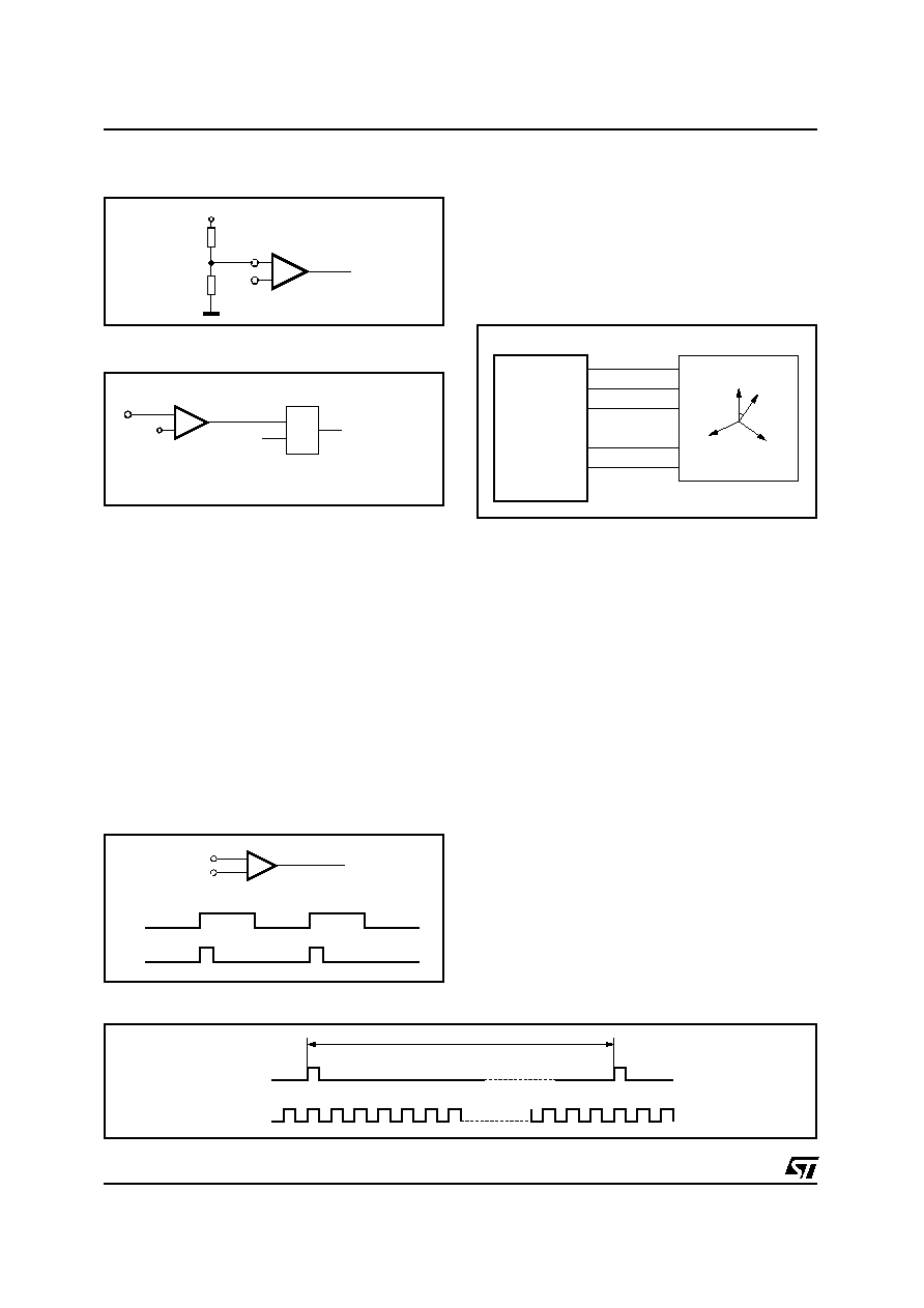
SMOOTH DRIVE
TM
SYSTEM
1.8A DRIVE PEAK CAPABILITY
SLEW RATE CONTROL
INDUCTIVE SENSE START-UP ROUTINE
THERMAL SHUTDOWN
SUITABLE FOR 5V AND 12V APPLICATION
ONLY ONE HALL SENSOR IS REQUIRED
DESCRIPTION
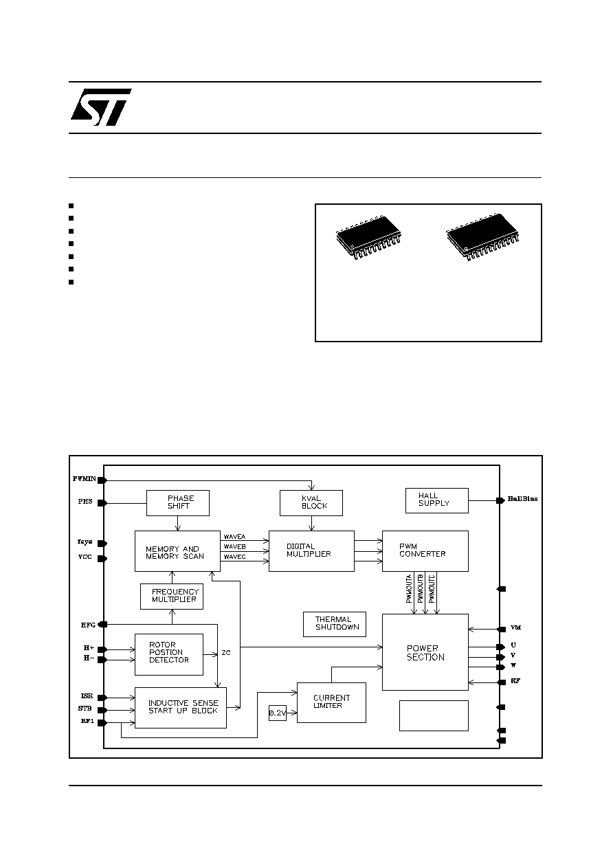
The L7203 SPINDLE MOTOR IC includes a three
phase brushless spindle motor controller and the
power stage in switching mode. The device is de-
signed for both 5V and 12V OPTICAL DRIVE ap-
plication requiring up to 1.8A peak of current.
The device is realized in BCD5, a 0.7
µ
m Mixed
technology.
The spindle motor position detection is carried
out by means of a single comparator with hyster-
esis. In the start-up phase the "inductive sense
start up method" is used to detect the rotor posi-
tion, determining the direction of starting rotation.
This procedure is implemented by a logic circuit
on chip.
The device applies three sinusoidal voltages to
the motor coils.
This is obtained through the application of the
April 2001
LOW VOLTAGE
DETECTOR
PRS
SRC
AGND
DGND
BLOCK DIAGRAM
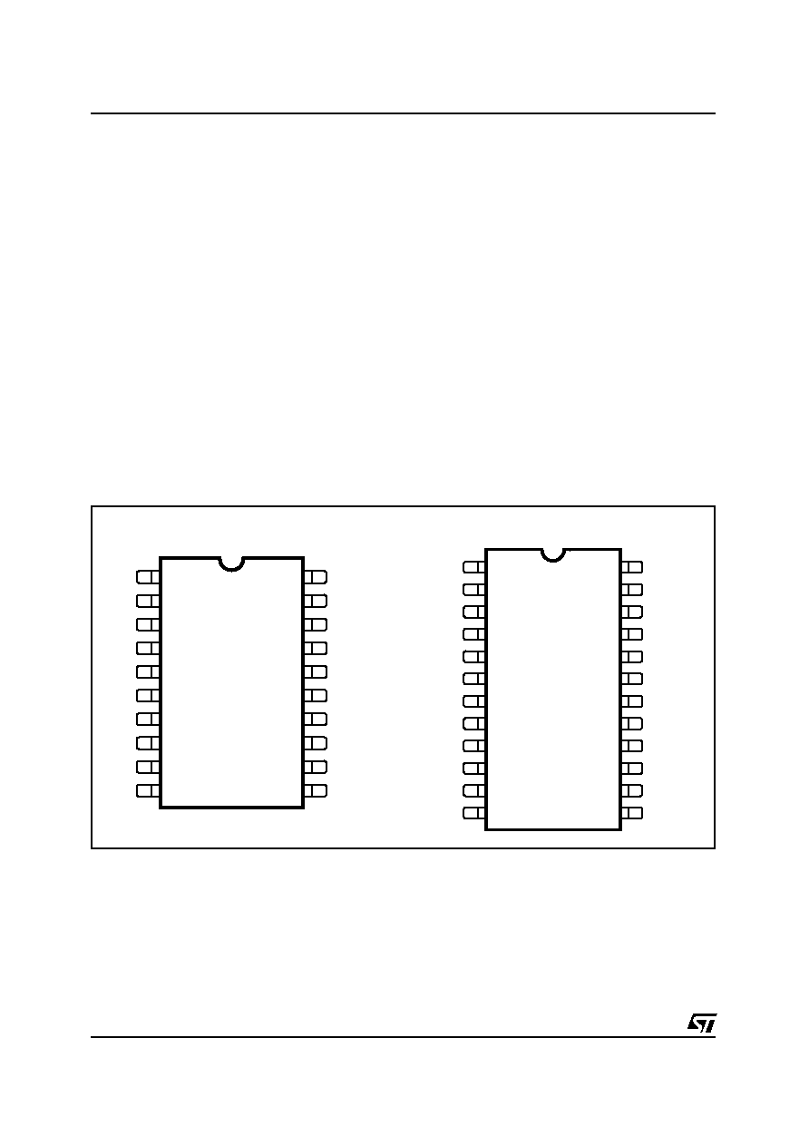
ORDERING NUMBERS: L7203 (SO20)
L7203S (SSO24)
L7203
SMOOTH DRIVE SPINDLE MOTOR FOR OPTICAL DRIVE
APPLICATION WITH POWER INTEGRATED
®
SO20
SSO24
1/13
SMOOTH DRIVING concept.
It is based on the idea of driving the motor wind-
ing through 3 sinusoidal voltages dephased of
120 degrees. The motor is controlled in voltage
mode, so no current control compensation net-
work is required.
Each profile is digitally described by 36 bytes
stored in a ROM memory.
These sinusoidal signals are modulated by multi-
plying each sample by a value stored in the KVAL
register. Using this kind of profiles it is possible to
obtain great advantages such as torque ripple
and acoustic noise reduction and lower EMI. An
easier track following is ensured, since vibration
are reduced.
The clock signal on the chip can be synchronized
to the external application clock signal.
An internal circuit can limit the current. The
threshold is fixed with a internal 0.2 V reference.
The device generates:
- a current generator to define output voltage
slew rate
- a 3.3 V reference to bias hall sensor.
- the HFG open drain output signal for speed
regulation.
The device includes :
- a circuit for thermal shutdown with hysteresis.
- a low voltage detector
In the STANDBY state the main functions of the
device are turned off, in order to minimize the
power consumption.
The STANDBY state of the device is imposed by:
- Thermal shutdown
- stand by signal from
µ
P
PIN CONNECTIONS
DESCRIPTION (continued)
PRS
N.C.
N.C.
VM
U
N.C.
V
W
RF
H BIAS
ISR
V
CC
DGND
AGND
SRC
HFG
FSYS
STB
1
3
2
4
5
6
7
8
9
22
21
20
19
18
16
17
15
23
10
24
N.C.
PHS
D01IN1174
RF1
PWMIN
11
14
13
12
H+
H-
STB
PRS
VM
U
V
RF
W
RF1
H+
PHS
HBIAS
ISR
AGND
VCC
DGND
SRC
HFG
FSYS
1
3
2
4
5
6
7
8
9
18
17
16
15
14
12
13
11
19
10
20
H-
PWMIN
D98IN928A
SO20
SSO24
L7203
2/13

PIN DESCRIPTION
PIN
DESCRIPTION
TYPE
POWER AND GROUND
VM
Supply voltage for power stages +12/5V
P12
VCC
Supply for 5V core
P5
DGND
Logic ground
G
AGND
Analog ground
G
DIGITAL PIN
PWMIN
PWM input signal to calculate kval
IC5
Fsys
System frequency
IC5
PHS
Phase Shift Pin
IC5
PRS
Prescaler Pin
IC5
STB
Start and Stop signal
ZD5
HFG
Open Drain F-Generator signal from Spindle Motor
OD5
HALL SENSOR
BIAS
3.3V reference to bias Hall sensor
OA5
H+, H-
Hall sensor differential input
IA5
INDUCTIVE SENSE REFERENCE
ISR
Inductive sense reference
IA5
MOTOR CONTROL
OUTV
Winding output U
OA12
OUTV
Winding output V
OA12
OUTW
Winding output W
OA12
RF
Current sense resistor (force)
OA12
RF1
Current sense resistor (sense)
IA5
SLEW RATE CONTROL
SRC
Slew Rate Control
OA5
INPUT DEFINITION
IC5 Input CMOS, 3.3-5V capability with hysteresis
ZD5 Bidirectional, open drain, 3.3-5V capability
OD5 Output, open drain, 3.3-5V capability
IA5 Input, Analog, 5V
OA5 Output, Analog, 5V
OA12 Output, Analog, 12V
P12 Power 12V / 5V
P5 Power 5V
G Ground
L7203
3/13
DC ELECTRICAL CHARACTERISTICS ( V
CC
= 5V; V
M
= 12V; T
amb
= 25°C unless otherwise specified)
Symbol
Parameter
Test Condition
Min.
Typ.
Max.
Unit
SUPPLY
V
CC
Supply 5V operating range
4.25
5.75
V
V
M
Supply 12V operating range
(note 1)
10.2
13.8
V
V
M
Supply 5V operating range
4.25
5.75
V
I
Vcc
V
CC
Supply Current
V
CC
= 5.75; f
sys
= 20MHz STB = 0
(bias pin open) STB =1
1.3
20
mA
mA
V
VM
V
M
Supply Current
V
M
= 13.8 STB = 0
STB =1
1
7
mA
mA
PWMIN, PHS, PRS, Fsys
V
iL
Input Low Voltage
1
V
V
iH
Input High Voltage
2.2
V
V
iHYS
Input Hysteresis
100
mV
I
z
Leakage Current
V
CC
= 5.75
-10
+10
µ
A
STB
V
iL
Input Low Voltage
1
V
V
iH
Input High Voltage
2.2
V
V
OL
Open Drain Output
IOL = 2mA V
CC
= 4.25V
0.4
V
V
iHYS
Input Hysteresis
100
mV
I
z
Leakage Current
V
CC
= 5.75, Therm off
-10
+10
µ
A
HFG
V
OL
Open Drain Output
IOL = 2mA V
CC
= 5V
0.4
V
I
z
Leakage Current
V
CC
= 5.75, HFG hiz
-10
+10
µ
A
THERMAL DATA
Symbol
Parameter
Value
Unit
R
th j-pins
Thermal Resistance Junction to Pins Max.
16
°C/W
R
th j-amb
Thermal Resistance Junction to Ambient Max.
90
°C/W
ABSOLUTE MAXIMUM RATINGS
Symbol
Parameter
Value
Unit
T
amb
Ambient Temperature
-20 to 80
°C
T
op
Operating Temperature
0 to 150
°C
T
smin
Minimum Thermal Circuit Threshold
140
°C
V
M
-0.3 to 15
Vdc
V
CC
-0.3 to 7
Vdc
U, V, W, (low side drive =off)
-0.3 to 17
Vdc
PWMIN, PHS, FSYS, TEST, STB, HFG, BIAS, H+, H-, RF1,
RF, ISR, PORPin
-0.3 to V
CC
+0.3
Vdc
P
D1
Power dissipation at sustained operation with a package R
thj-amb
at 90°C
1
W
ESD
Susceptibility
2000
Vac
T
STG
Storage Temperature
-55 to 150
°C
I
OLHFG
HFG open drain current
10
mA
I
Peak
Motor Peak Current
1.8
A
L7203
4/13
FUNCTIONAL DESCRIPTION
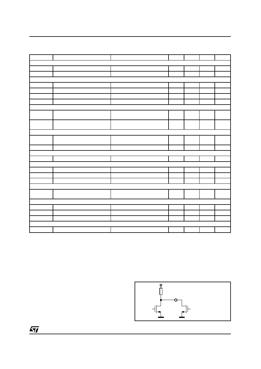
STB-Thermal protection
Controller drive STB pin by open drain.
When Thermal Shutdown is excited, the device
force this pin LOW.
Controller will manage STB to do a re-start.
When STB is LOW all the drivers are shut off.
Hall Sensor Bias
A regulator on chip supply a 3.3V+-10% refer-
ence on pin Bias. This regulator can supply an
output current up-to 15 mA.
Symbol
Parameter
Test Condition
Min.
Typ.
Max.
Unit
BIAS
V
BIAS
BIAS Output Voltage
V
CC
= 5V; 5mA < I < 15mA
3.25
3.75
V
I
Bmax
Max Output Current
15
mA
H+, H-
V
H
±
H+ H- Input Voltage Range
0
2.5
V
I
H
±
Input Leakage Current
V
in
= 0, +V
CC
-10
+10
µ
A
V
OFFISR
Comparator Offset
-15
+15
mV
VHy
Comparator Hysteresys
4
15
mV
MOTOR POWER STAGE
R
DSON
High and Low side FET on
Resistance
T
j
= 125; V
M
= 4.25V
I = 1.2A
2
I
U/V/W
Spindle Output Leakage
Current
V
M
= 15V
100
µ
A
CURRENT LIMITER
V
Lim
Internal Reference Voltage for
current limitation
220
240
260
mV
V
OFFLim
Comparator Offset
-15
+15
mV
THERMAL PROTECTION
T
S
Shutdown temperature
130
170
°C
UNDERVOLTAGE
V
ccth (fall)
Undervoltage threshold (fall)
2.9
-
-
V
V
ccth (rise)
Undervoltage threshold (rise)
-
-
3.4
V
V
ccth (hys)
Undervoltage threshold (hys)
-
0.1
-
V
SYSTEM FREQUENCY
f
sys
System frequency
PRS = 0
PRS = 1
10
20
20
34
MHz
MHz
SLEW RATE CONTROL
V
SRC
SRC Output Voltage
1.25
V
I
SRC
Output Current
500
µ
A
R
SRC
External Resistor on pin SRC
10
K
ISR
V
ISR
Input Range
0
2
V
Note 1: An SMBJIZAVCL-TR is recommended to clamp V
M
in case of high impedance on power supply line.
DC ELECTRICAL CHARACTERISTICS (continued)
R PULL UP
OVER TEMP
STB
D98IN880
Figure 1.
L7203
5/13
Inductive Sense Start Up Block
The inductive sense method allows to determine
the position and the direction of the starting rota-
tion of the motor.
With the rotor at rest, a voltage Vn is applied sub-
sequently to two motor phases, according to this
sequence: UW, VW, VU, WU, WV, UV.
A timer measures the rise time dT to reach the
reference current ISR in each phase.
This reference is fixed on the pin ISR with a resis-
tor divider between the pin BIAS and GND.
Through a comparator is possible to determine
the phase which has the minimum rise time and
so the rotor position is univocally determinated.
The start up is a procedure allowing to start the
motor avoiding any backrotation. This procedure
is realized by a customized logic on chip (no
modification required in the external microproces-
sor software).
For the Motor Connection please refer to the Fig. 4.
Current Limiter
The current limiter aim is to avoid that the current
in the motor winding overides a fixed threshold
value. The voltage input at the pin RF1 is com-
pared with an internal 0.2V reference.
When the current exceeds the Ilimit value a flip-
flop is reset masking (through a combinational
logic) the signal to the power windings.
Rotor Position Detector
This block is connected to the Hall Sensor Out-
put. A comparator with hysteresis receives the
sinusoidal hall-sensor signal and generates a
squared signal HOUT.
The Zero-Cross signal is generated starting from
the HOUT signal as in fig. 5.
The HOUT signal can be read from the micro-
processor on the output open drain pin HFG.
Frequency multiplier
The Frequency Multiplier generates the memory
scan frequency (Fscan) starting from the Zero-
Cross (ZC) signal from the Rotor Position Detec-
tor block. The scan frequency relates to the rate
of the samples of the input signals.
The number of wave samples in a period T is 36,
so this circuit generates 36 pulses between 2
Zero Crossing.
CURRENT LIMIT
RF1
D98IN882
0.2V
-
+
R
S
TO THE POWER STAGE
SET EVERY
255 CLOCK
CYCLE
INTERNAL
REFERENCE
Figure 3.
HOUT
H+
D98IN883A
-
+
COMPARATOR WITH HYSTERESIS
H-
HOUT
ZC
Figure 5.
T
ZC
Fscan
1
2
3
4
5
6
7
8
35
36
D98IN879
Figure 6.
R1
TIMER
ISR
D98IN881
BIAS
RF1
R2
-
+
Figure 2.
L7203
30°
Bemf coil B
Hall sensor
Bemf coil C
Bemf coil A
MOTOR COIL A
MOTOR COIL B
MOTOR COIL C
U
V
W
H+
H-
H+
H-
MOTOR
D01IN1175
Figure 4. Motor Connections.
L7203
6/13

Fscan has a frequency 36 times of (1/T). The
Fscan is generated from the Zero-cross fre-
quency measured at the previous cycle.
So, if the motor speed changes, the zero-cross is
not constant, the Frequency Multiplier adjusts the
scan clock, ensuring the synchronization between
the Zero-Cross signal and the sinusoidal output
voltage.
Memory and Memory Scan
The memory stores 3x36 samples describing 3
signals. As each sample is represented in a byte,
it may have a value in the range 0 to 255.
The shape of these three signals are designed in
order to generate three sinusoidal voltages
across the Motor coils ensuring the highest per-
formances in term of power losses and motor
speed. The shape of the signals are reported in
fig. 7.
In Fig 8 is swown the "differential" voltage across
the motor coil U and the motor coil V. Obviously,
the voltage shape across the motor coil U and W
and the voltage across the motor coil V and W
are also sinusoidal and dephased of 120 and 240
degrees respect the voltage shown in fig. 8.
The Memory and Memory scan block receives
the scan clock, and at each clock provides the
sample addressed by an internal address regis-
ter.
This register is initialized with the memory ad-
dress of the wave sample synchronized with the
Zero-Cross signal. The maximum efficiency (i.e.
the maximum motor speed for a particular value
of current) for the motor driving may be reached
ensuring a particular value PH of dephase be-
tween the Zero-Cross signal and the voltage out-
put signal.
This value is written by the external controller us-
ing PHS pin (see Phase Shift Block section).
Kval Block and PWM interface
This unit contains a register storing the Kval
value. The Kval value represents a multiplying
factor to modulate the 3 profile signals amplitude
and it is generated starting from the PWMIN sig-
nal coming from the external system controller.
The Kval block receives the PWMIN signals and
calculates the Kval value through the reference
triangular signal.
This signal is generated by a 10 bit counter that
starts counting from 1023 to 0 at Fsys rate, and
then restart up to 1023. The resolution is
±
1LSB.
Internal triangular wave is synchronized with the
PWMIN falling edge.
The PWMIN signal contains information regard-
ing both the amplitude and to the sign of the con-
trol variable. If the duty cycle is less than 50% the
Kval is in the range (-1023, -1), while if the duty
cycle is equal or greater than 50% the kval is in
the range (0, 1023).
A negative Kval value (i.e. PWM duty cycle from
0 to 50%) indicates an active brake and gener-
ates a 180 degree shift in the voltage profile
scan.
The rising edge of the PWMIN signal determines
the kval on the reference triangular waveform.
If the PWMIN signal is stable during the entire cy-
cle, the Kval is evaluated according to the follow-
ing rule:
- PWMIN signal stable to 1 -> Kval = +1023
- PWMIN signal stable to 0 -> Kval = -1023
In order to ensure the synchronization between
INTERNAL
REFERENCE
SIGNAL
PWMIN
0
1023
KVAL < 0
KVAL > 0
KVAL < 0
D98IN884
Figure 9.
U-W
D98IN931
Figure 8.
V
U
W
D98IN930
Figure 7.
L7203
7/13

the PWMIN signal and the internal signals, the
PWMIN signal rate must be calculated by the ex-
ternal microcontroller using the same frequency
signal provided to the chip through the pin fsys.
Digital Multiplier
This unit contains a multiplier executing the multi-
plication of each sample provided by the memory
by the value stored in kval register.
The output value is a 10-bit word, plus the sign bit.
PWM Converter
The PWM converter receives from the digital mul-
tiplier three 10 bit digital number and converts it
into three PWM signals.
A counter counts up (from 0 to 255) and down
(from 255 to 0) at the Fsys rate in continuos
mode. Three 8-bit input registers are written with
the 8 most significant bit of the word to be con-
verted and compared to the counter value. The
comparator output is:
COMPARATOR
8 MSB
OUTPUT MULTIPLIER
D98IN886
OUTPUT
OUTPUT PWM:
LSB
00
01
10
11
WHERE:
A HALF FSYS PERIOD
A FSYS PERIOD
Figure 11.
COUNTER
OUTPUT COMPARATOR
0
255
D98IN885A
510 Tsys
Figure 10.
L7203
8/13

- 0, if the input value is smaller than the counter
output
- 1, if the input value is equal or greater than the
counter output
The comparator output is "adjusted" with a com-
binational logic with the 2 low significant bit of the
word to be converted in order to reach a 10 bit
precision.
The comparator output duty cycle is extended
with a half fsys period for every low bit step how
is showed in the figure 11.
Phase Shift Block
This block regulates the phase of the driving sig-
nal to control the dephasing between the Zero-
Cross signal and the voltage sinusoidal output
signal.
It is possible to demonstrate that the maximum
efficiency for the motor driving may be reached
ensuring a particular value PH of dephase be-
tween the Zero-Cross signal and the voltage out-
put signal.
The Phase Shift BLock, starting from the PHS in-
put signal synchronize the wave output with the
Zero-Cross signal to ensure the optimum
dephase.
The PHS signal expresses the phase shift
through the duration of its value according to the
following rule:
Table 1.
PHS on
NPhase
Phase Shift (degree)
time
µ
s (Tsys = 50ns)
decimal
bit
0
0.2
0.4
0.6
0.8
1.0
1.2
1.4
0
1
2
3
4
5
6
7
00000 000
00000 001
00000 010
00000 011
00000 100
00000 101
00000 110
00000 111
LATCH
1.25
2.50
3.75
5.00
6.25
7.50
8.75
1.6
1.8
2.0
2.2
2.4
2.6
2.8
3.0
8
9
10
11
12
13
14
15
00001 000
00001 001
00001 010
00001 011
00001 100
00001 101
00001 110
00001 111
10
11.25
12.50
13.75
15.00
16.25
17.50
18.75
3.2
3.4
3.6
3.8
4.0
4.2
4.4
4.6
16
17
18
19
20
21
22
23
000010 000
000010 001
000010 010
000010 011
000010 100
000010 101
000010 110
000010 111
20
21.25
22.50
23.75
25.00
26.25
27.50
28.75
.
.
.
.
.
.
.
.
.
.
.
.
16.0
16.2
16.4
16.6
16.8
17.0
17.2
17.4
80
81
82
83
84
85
86
87
001010 000
001010 001
001010 010
001010 011
001010 100
001010 101
001010 110
001010 111
100
101.25
102.50
103.75
105.00
106.25
107.50
108.75
.
.
.
.
.
.
.
.
.
.
.
.
L7203
9/13
PHS on = tsys * 4 * Nphase
where: tsys = 50ns if fsys = 20MHz
The resulting PHASE SHIFT value is:
PHASE SHIFT = Nphase(8:3) x 10 +
Nphase(2:0) x 1.25
For istance if Nphase = 00011 110
PHASE SHIFT = 3 x 10 + 6 x 1.25 = 37.5
Low Voltage Detector
This circuit detects if V
CC
is lower than a fixed
threshold. If this event happens the internal logic
is resetted and the output FETS are forced in
High impedance.
Slew Rate Control Circuit
This circuit fixes the slew rate for the output stage
in order to reduce EMI.
A reference current is generated by means of an
internal reference voltage and an external resis-
tor.
The I
SRC
is used to fix slew rate with a linear law:
SLEW RATE = R
SLR/ISRC
V
REF
R
EXT
R
ext
recommended value >10K
Prescaler Pin
The PRS Pin should be forced to ground when
the FSYS frequency is lower (or equal) than
20MHz and should be forced to V
CC
when FSYS
frequency is higher than 20MHz, in order to set
the correct timing during the inductive sense,
start up and resynchronization phases.
Example of different phase shift settings are
shown in the following pictures.
PHS on
NPhase
Phase Shift (degree)
time
µ
s
decimal
bit
56.0
56.2
56.4
56.6
56.8
57.0
57.2
57.4
> 57.6
280
281
282
283
284
285
286
287
288
100011 000
100011 001
100011 010
100011 011
100011 100
100011 101
100011 110
100011 111
100100 000
350
351.25
352.50
353.75
355.00
356.25
357.50
358.75
0
Table 1. (continued)
V
REF
V
REF
I
SRC
=
SRC
R
ext
/
R
ext
+
-
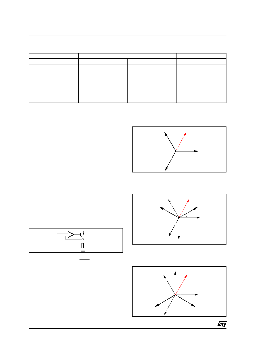
Figure 12.
Hall sensor
OUT V
OUT U
OUT W
Figure 13. Phase relation between OUTPUT
sinusoidal voltage (PWM_IN > 50%)
and Hall sensor signal writin Phase
shift = 0° (default value)
Hall sensor
OUT V
OUT U
OUT W
30°
Figure 14. Phase relation between OUTPUT
sinusoidal voltage (PWM_IN > 50%)
and Hall sensor signal writing Phase
shift = 30°
Hall sensor
30°
OUT V
OUT U
OUT W
Figure 15. Phase relation between OUTPUT
sinusoidal voltage (PWM_IN > 50%)
and Hall sensor signal writing Phase
shift = 330°
L7203
10/13
1
1
0
11
20
A
e
B
D
E
L
K
H
A1
C
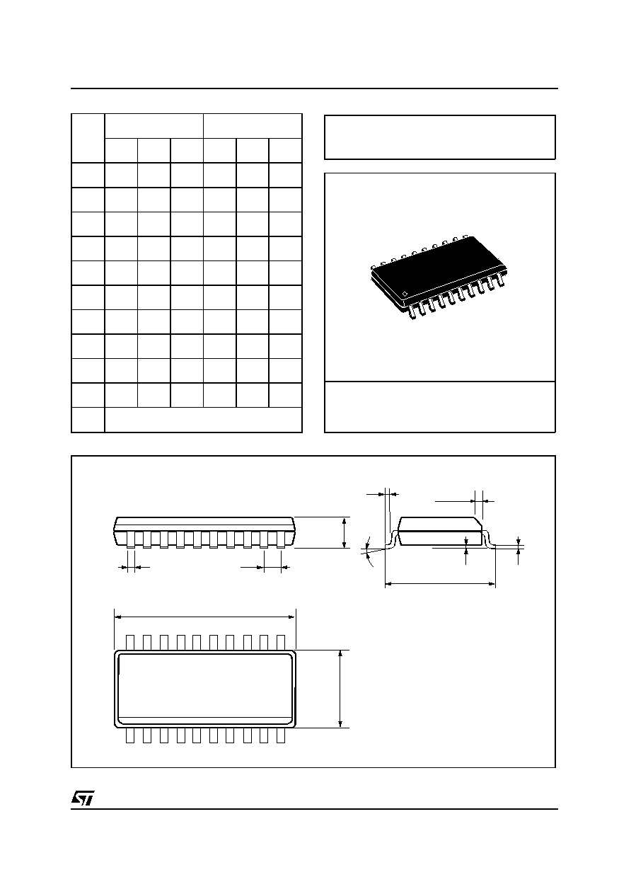
SO20MEC
h x 45°
SO20
DIM.
mm
inch
MIN.
TYP.
MAX.
MIN.
TYP.
MAX.
A
2.35
2.65
0.093
0.104
A1
0.1
0.3
0.004
0.012
B
0.33
0.51
0.013
0.020
C
0.23
0.32
0.009
0.013
D
12.6
13
0.496
0.512
E
7.4
7.6
0.291
0.299
e
1.27
0.050
H
10
10.65
0.394
0.419
h
0.25
0.75
0.010
0.030
L
0.4
1.27
0.016
0.050
K
0° (min.)8° (max.)
OUTLINE AND
MECHANICAL DATA
L7203
11/13
OUTLINE AND
MECHANICAL DATA
DIM.
mm
inch
MIN.
TYP.
MAX.
MIN.
TYP.
MAX.
A
2.00
0.079
A1
0.05
0.002
A2
1.65
1.75
1.85
0.060
0.079
B (2)
0.22
0.38
0.009
0.015
C
0.09
0.25
0.003
0.01
D (1)
7.9
8.2
8.5
0.31
0.32
0.33
E
7.4
7.8
8.2
0.29
0.30
0.32
E1 (1)
5.0
5.3
5.6
0.20
0.21
0.22
e
0.65
0.025
L
0.55
0.75
0.95
0.022
0.029
0.004
L1
1.25
0.05
k
0° (min), 4° (typ), 8° (max)
ddd
0.1
0.004
(1) "D and E1" dimensions do not include mold flash or protu-
sions, but do include mold mismatch and are mesaured at
datum plane "H". Mold flash or protusions shall not exceed
0.20mm in total (both side).
(2) "B" dimension does not include dambar protusion/intrusion.
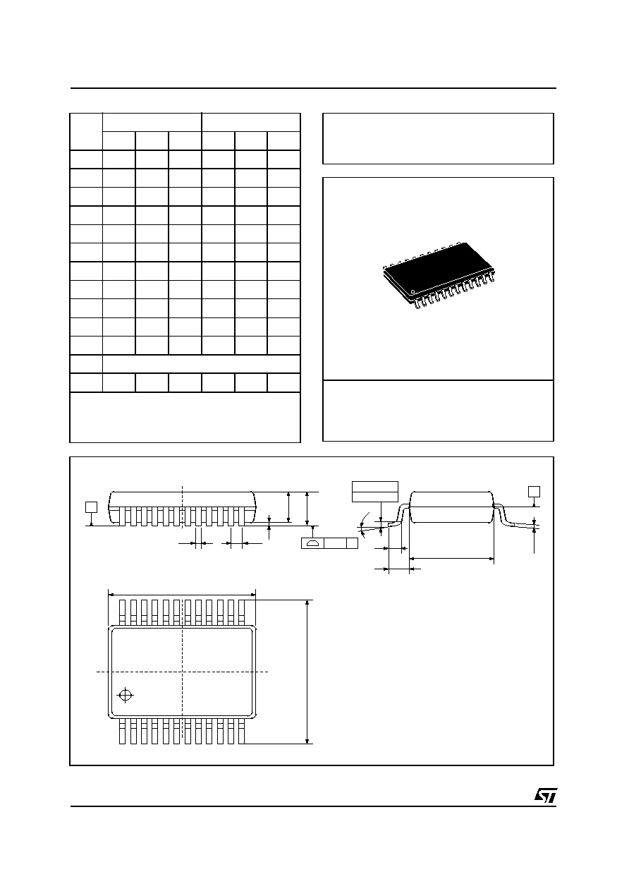
SSO24
0053237
B
e
A2
A
1
1
2
13
24
D
L
L1
E1
C
E
K
SSO24ME
SEATING
PLANE
C
A1
ddd
C
0.25mm
GAGE PLANE
DATUM
PLANE
H
Shrink Small Outline Package
L7203
12/13

Information furnished is believed to be accurate and reliable. However, STMicroelectronics assumes no responsibility for the consequences
of use of such information nor for any infringement of patents or other rights of third parties which may result from its use. No license is
granted by implication or otherwise under any patent or patent rights of STMicroelectronics. Specification mentioned in this publication are
subject to change without notice. This publication supersedes and replaces all information previously supplied. STMicroelectronics products
are not authorized for use as critical components in life support devices or systems without express written approval of STMicroelectronics.
The ST logo is a registered trademark of STMicroelectronics
© 2001 STMicroelectronics Printed in Italy All Rights Reserved
STMicroelectronics GROUP OF COMPANIES
Australia - Brazil - China - Finland - France - Germany - Hong Kong - India - Italy - Japan - Malaysia - Malta - Morocco -
Singapore - Spain - Sweden - Switzerland - United Kingdom - U.S.A.
http://www.st.com
L7203
13/13