®
1/7
EMIF04-MMC02F2
4 LINES EMI FILTER
INCLUDING ESD PROTECTION
REV. 2
April 2005
IPADTM
Flip-Chip
(11 Bumps)
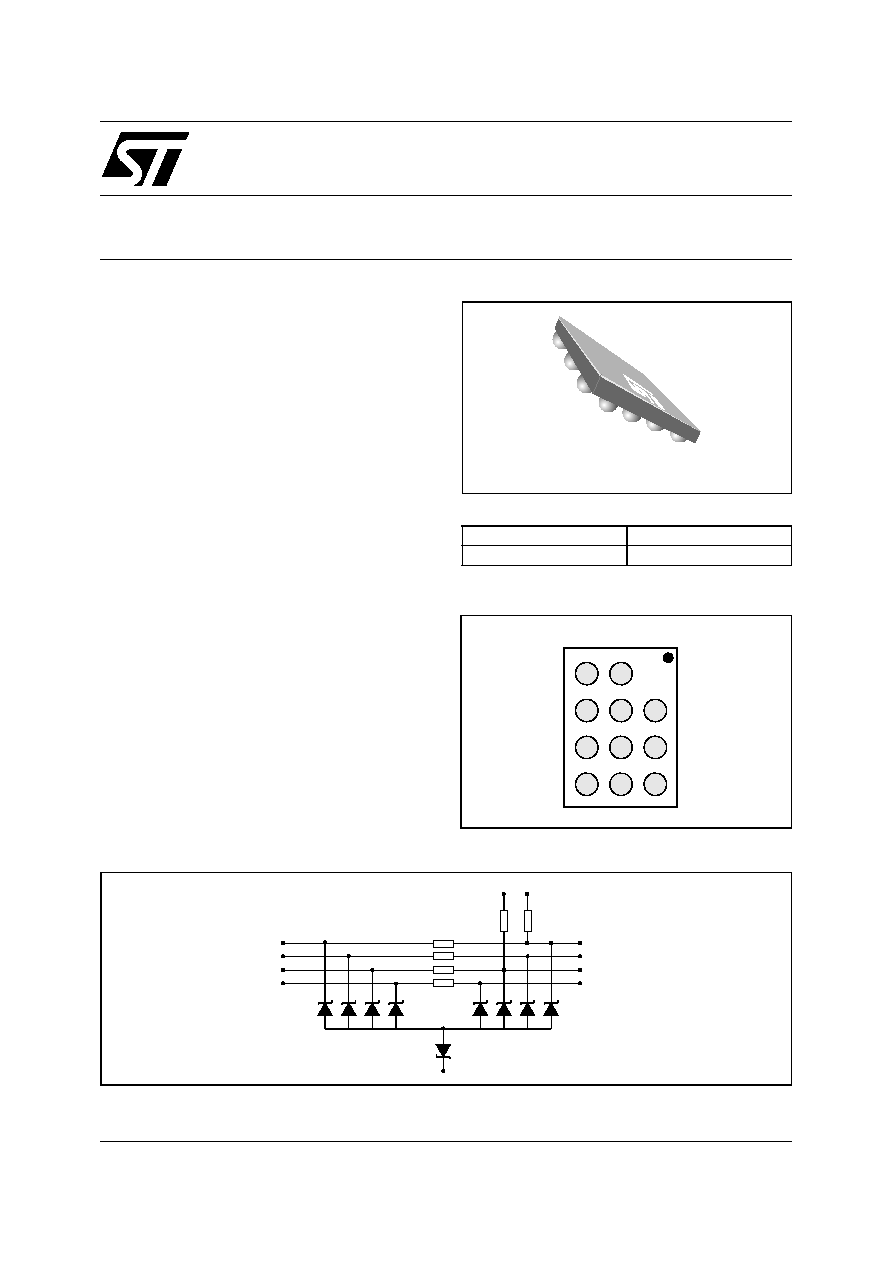
Figure 1: Pin Configuration (ball side)
O1
I4
GND
VD1
O4
O3
O2
I3
I2
VD2
I1
B
1
2
3
C
D
A
TM: IPAD is a trademark of STMicroelectronics.
Table 1: Order Code
Part Number
Marking
EMIF04-MMC02F2
FH
MAIN PRODUCT CHARACTERISTICS:
Where EMI filtering in ESD sensitive equipment is
required:
MultiMedia Card for mobile phones, Personal
Digital Assistant, Digital Camera, MP3 players...
DESCRIPTION
The EMIF04-MMC02 is a highly integrated devic-
es designed to suppress EMI/RFI noise for Multi-
Media Card port. The EMIF04 flip chip packaging
means the package size is equal to the die size.
This filter includes an ESD protection circuitry
which prevents the device from destruction when
subjected to ESD surges up 15kV.
BENEFITS
EMI symmetrical (I/O) low-pass filter
High efficiency in EMI filtering
Lead free package
Very low PCB space consuming:
1.57 mm x 2.07 mm
Very thin package: 0.65 mm
High efficiency in ESD suppression
High reliability offered by monolithic integration
High reducing of parasitic elements through
integration & wafer level packaging.
COMPLIES WITH THE FOLLOWING STANDARDS:
IEC61000-4-2
Level 4
15kV (air discharge)
8kV (contact discharge)
Figure 2: Configuration
GND
Cline = 20pF max.
I1
I2
I3
I4
O1 (Data)
O2 (CLK)
O3 (CMD)
O4
R1
R2
R3
R4
R20
R10
VD2
VD1

EMIF04-MMC02F2
2/7
Table 2: Absolute Ratings (T
amb
= 25°C))
Table 3: Electrical Characteristics (T
amb
= 25°C)
Symbol
Parameter and test conditions
Value
Unit
P
R
DC power per resistor
70
mW
T
j
Maximum junction temperature
125
°C
T
op
Operating temperature range
- 40 to + 85
°C
T
stg
Storage temperature range
- 55 to + 150
°C
Symbol
Parameter
V
BR
Breakdown voltage
I
RM
Leakage current @ V
RM
V
RM
Stand-off voltage
V
CL
Clamping voltage
R
d
Dynamic impedance
I
PP
Peak pulse current
R
I/O
Series resistance between Input & Output
C
line
Input capacitance per line
Symbol
Test conditions
Min.
Typ.
Max.
Unit
V
BR
I
R
= 1 mA
6
V
I
RM
V
RM
= 3V
100
500
nA
C
line
@ 0V
20
pF
R
1
,R
2
,R
3
,R
4
Tolerance ± 5%
47
R
10
Tolerance ± 5%
13
k
R
20
Tolerance ± 5%
56
k
EMIF04-MMC02F2
3/7
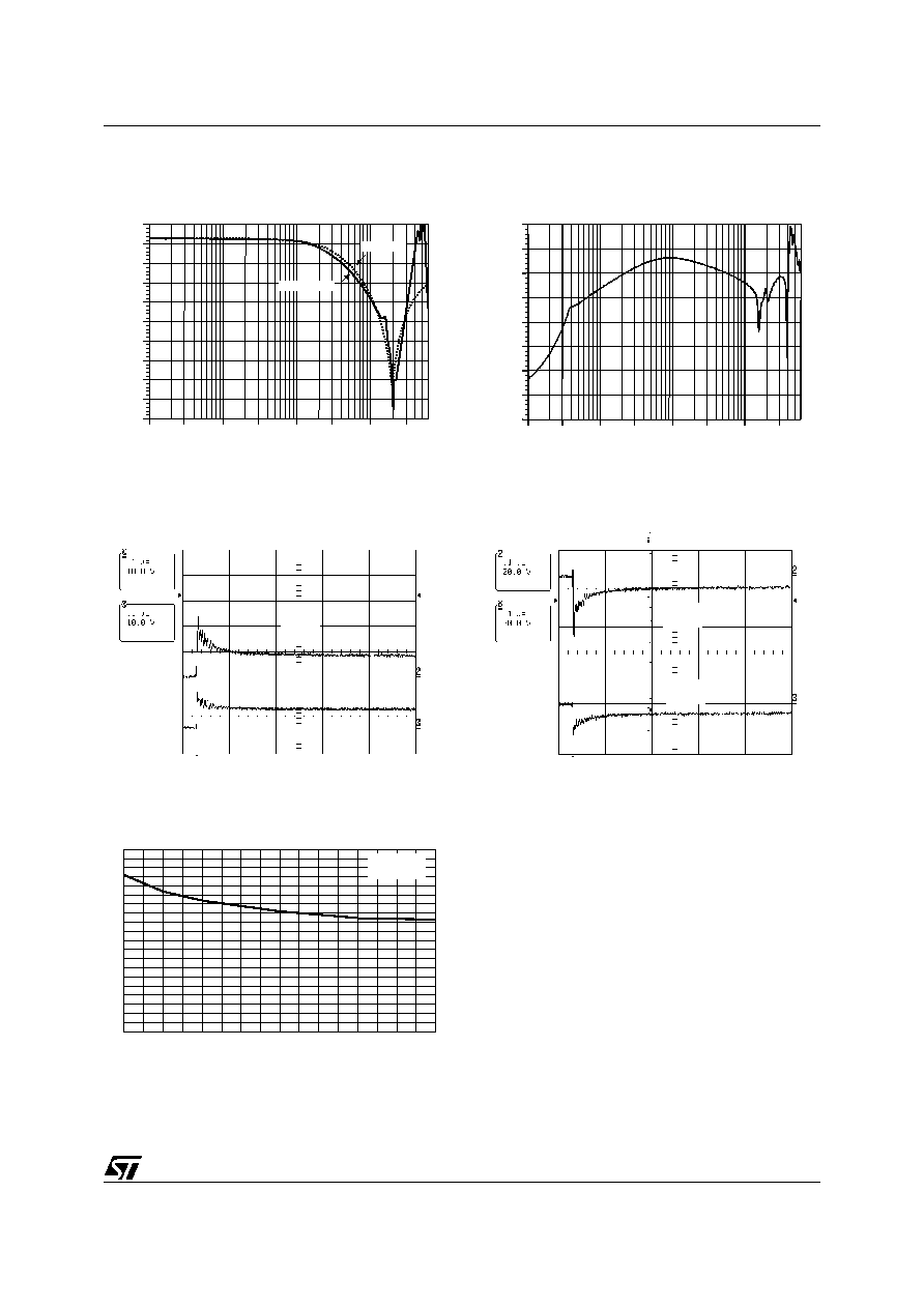
Figure 3: S21 (dB) attenuation measurement
and Aplac simulation
Figure 4: Crosstalk measurements
Figure 5: ESD response to IEC61000-4-2
(+15kV air discharge) on one input V(in) and on
one output (Vout)
Figure 6: ESD response to IEC61000-4-2 (-15kV
air discharge) on one input V(in) and on one
output (Vout)
Figure 7: Junction capacitance versus reverse
voltage applied (typical values)
1.0M
3.0M
10.0M
30.0M
100.0M
300.0M
1.0G
3.0G
- 50.00
- 45.00
- 40.00
- 35.00
- 30.00
- 25.00
- 20.00
- 15.00
- 10.00
- 5.00
0.00
EMIF04-MMC02F2: Aplac vs measurement (C3/C1 line)
dB
f/Hz
Measurement
-
-
Simulation
1.0M
3.0M
10.0M
30.0M
100.0M 300.0M
1.0G
3.0G
-80.00
-70.00
-60.00
-50.00
-40.00
-30.00
-20.00
-10.00
0.00
Xtalk measurements C3/B1
dB
f/Hz
V(in)
V(out)
V(in)
V(out)
0
2
4
6
8
10
12
14
16
18
20
0.0
0.5
1.0
1.5
2.0
2.5
3.0
3.5
4.0
V
R
(V)
C(pF)
F=1MHz
V
osc
=30mV
RMS
T
j
=25°C
EMIF04-MMC02F2
4/7
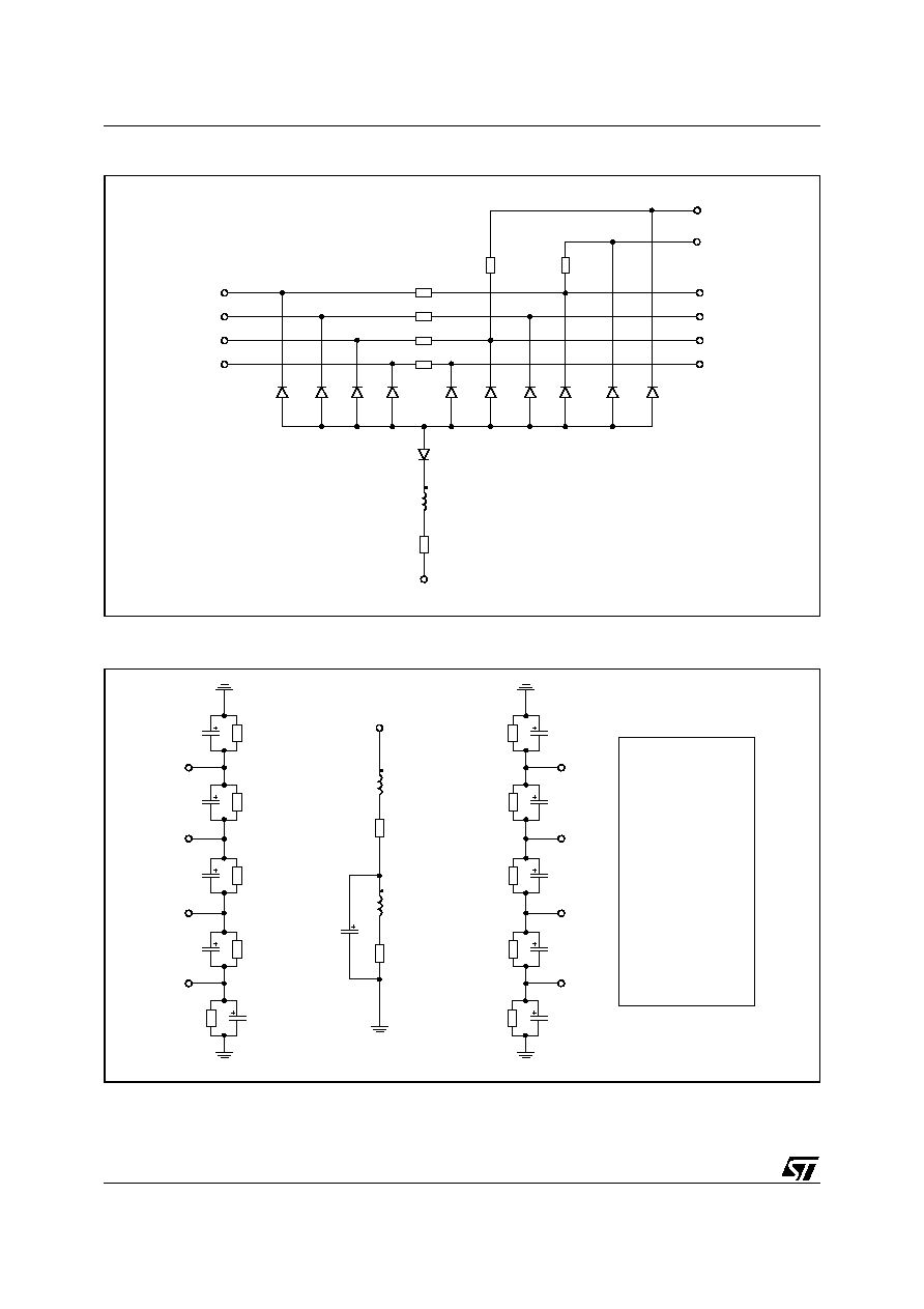
Figure 8: Aplac model device structure
Figure 9: Aplac model connections
R3
R2
R1
D1
C3
B3
A3
C1
B1
A2
120pH
100m
D3
C2
B2
R10
R20
MODEL = demif04_gnd
MODEL = demif04
MODEL = demif04
R4
D2
DEMIF04
BV = 7
IBV = 1m
CJO = Cz
M = 0.3333
RS = 1
VJ = 0.6
TT = 100n
DEMIF04 gnd
BV = 7
IBV = 1m
CJO = Cz_gnd
M = 0.3333
RS = 1
VJ = 0.6
TT = 100n
Lbump
Rbump
Lhole
Rhole
D2
cap_hole
Cins
Rins
A2
B1
C1
D1
Cins
Rins
Cins
Rins
Cins
Rins
Cins
Rins
Cins
Rins
A3
B3
C3
D3
Cins
Rins
Cins
Rins
Cins
Rins
Cins
Rins
Lbump 50pH
lhole 940pH opt
Rhole 100m
cap_hole 0.15pF
Cins 200fF
Rins 10Meg
R1 47 opt
R2 47
R3 47
R4 47
R10 13k
R20 56k
Cz 15pF opt
Cz_gnd 45pF opt
Ls 450pH opt
Rs 300m
Rbump 50m
EMIF04-MMC02F2
5/7
Figure 10: Order Code
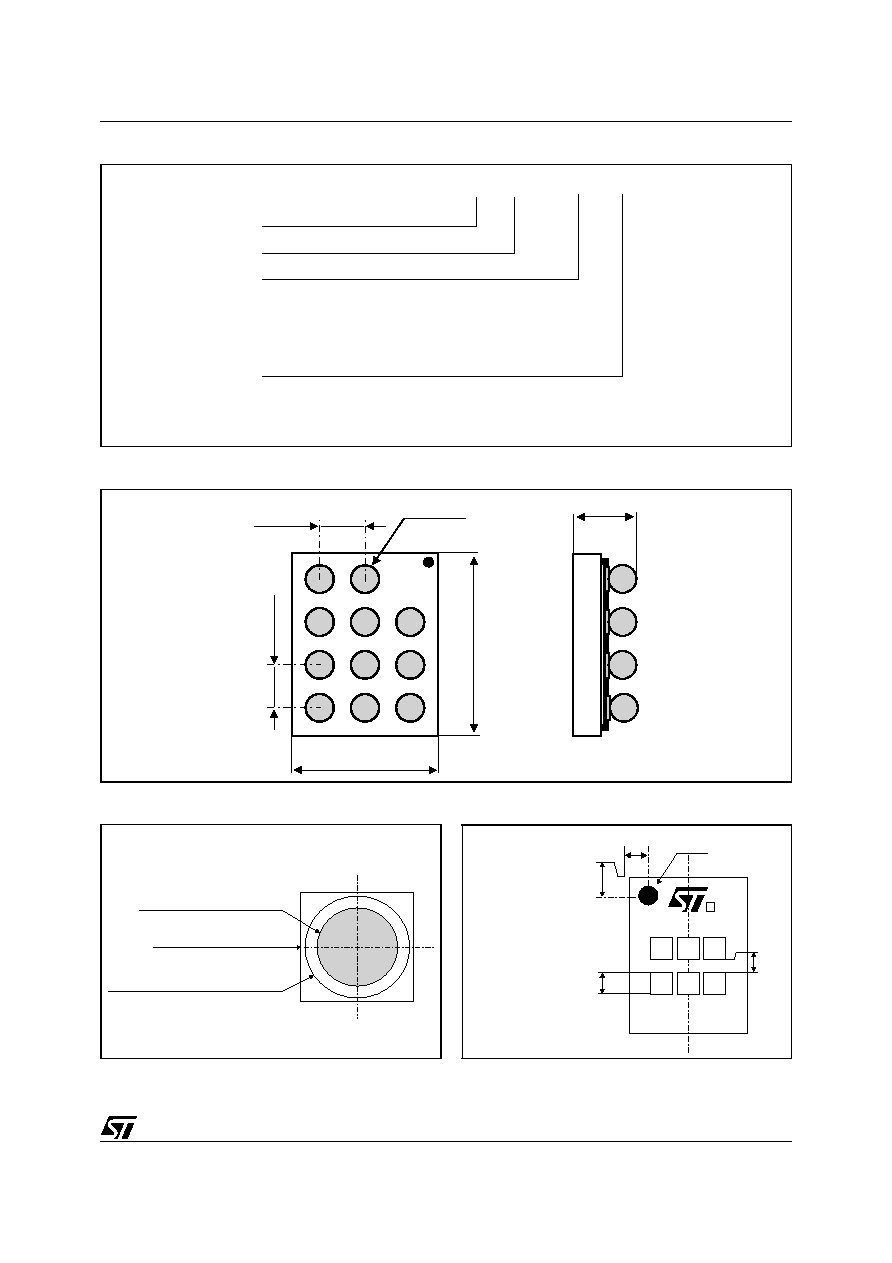
Figure 11: FLIP-CHIP Package Mechanical Data
Figure 12: Foot Print Recommendations
Figure 13: Marking
EMIF yy - xxx zz Fx
EMI Filter
Number of lines
Information
Package
x = resistance value (Ohms)
z = capacitance value / 10(pF)
or
3 letters = application
2 digits = version
F = Flip-Chip
x
= 1: 500µm, Bump = 315µm
= 2: Leadfree Pitch = 500µm, Bump = 315µm
= 3: Leadfree Pitch = 400µm, Bump = 250µm
1.57mm ± 50µm
2.07mm ± 50µm
315µm ± 50
500µm ± 50
500µm ± 50
650µm ± 65
Copper pad Diameter :
250µm recommended , 300µm max
Solder stencil opening : 330µm
Solder mask opening recommendation :
340µm min for 315µm copper pad diameter
545
545
400
100
230
x
y
x
w
z
w
E
All dimensions in µm
Dot, ST logo
xx = marking
yww = datecode
(y = year
ww = week)
z = packaging location