1/6
EMIF02-USB01
®
January 2003 - Ed: 5
IEC61000-4-2 level 4
15kV
(air discharge)
8 kV
(contact discharge)
on input & output pins.
COMPLIES WITH THE FOLLOWING STANDARDS :
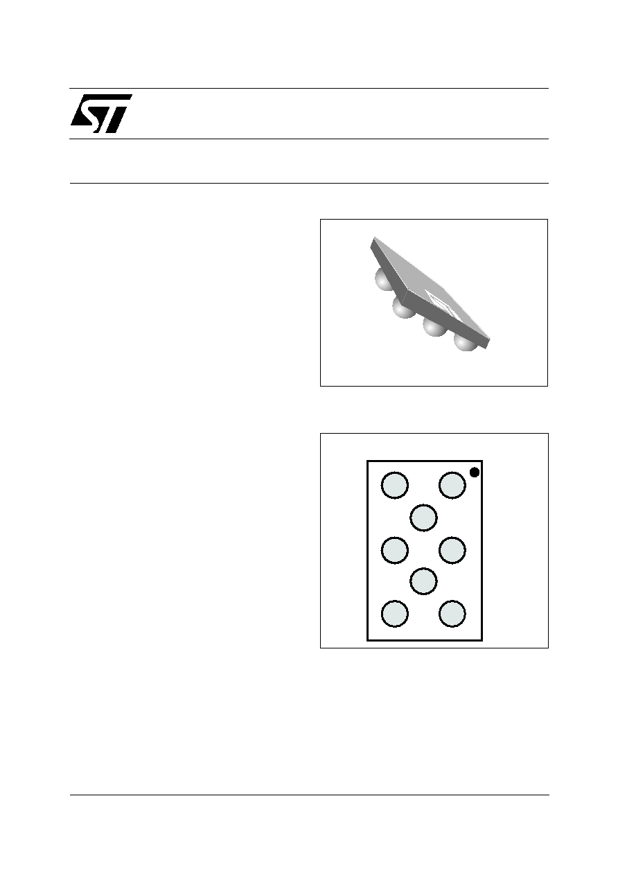
Flip Chip package
3
2
1
A
B
C
D
E
PIN CONFIGURATION
s
2 lines low-pass-filter + 2 lines ESD protection
s
High efficiency in EMI filtering
s
Very low PCB space consuming: 2.5 mm
2
s
Very thin package: 0.65 mm
s
High efficiency in ESD suppression
(IEC61000-4-2 level 4)
s
High reliability offered by monolithic integration
s
High reducing of parasitic elements through
integration & wafer level packaging.
BENEFITS
2 LINES EMI FILTER
INCLUDING ESD PROTECTION
IPAD
TM
s
ESD protection and EMI filtering for USB port.
MAIN APPLICATION
The EMIF02-USB01 is a highly integrated array
designed to suppress EMI / RFI noise for USB port
filtering.
The EMIF02-USB01 flip-chip packaging means
the package size is equal to the die size. That's
why EMIF02-USB01 is a very small device.
Additionally, this filter includes an ESD protection
circuitry which prevents the protected device from
destruction when subjected to ESD surges up to
15 kV.
DESCRIPTION
TM : ASD is trademark of STMicroelectronics.
EMIF02-USB01
2/6
D2
(gnd pin)
A1
B2
1.3K
C1
E1
E3
C3
A3
33R
33R
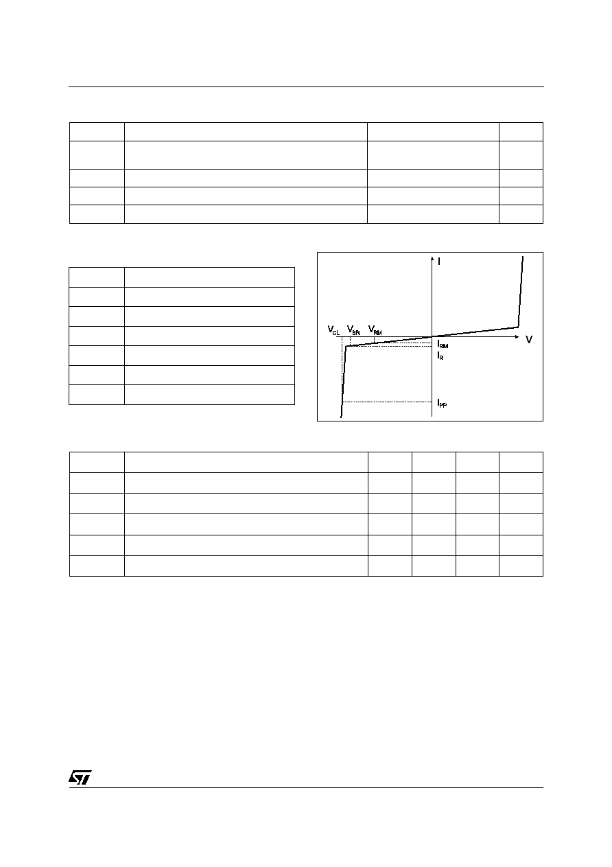
SCHEMATIC
1.0M
3.0M
10.0M
30.0M
100.0M
300.0M
1.0G
3.0G
-50.00
-45.00
-40.00
-35.00
-30.00
-25.00
-20.00
-15.00
-10.00
-5.00
0.00
EMIF02-USB01: filtering response of lines C1/C3 and E1/E3
dB
Frequency/Hz
0.00
C1_C3
E1_E3
Fig. 1: Filtering behavior
Vin
Vout
Fig. 2: ESD response to IEC61000-4-2 Level 4
10
15
20
25
30
35
40
0
0.5
1
1.5
2
2.5
3
3.5
4
4.5
5
VR (V)
C (pF)
Fig. 3: Capacitance versus reverse applied
voltage
1.0M
3.0M
10.0M
30.0M
100.0M
300.0M
1.0G
3.0G
-100.0
-90.00
-80.00
-70.00
-60.00
-50.00
-40.00
-30.00
-20.00
-10.00
0.00
dB
f/Hz
Fig. 4: Digital crosstalk
EMIF02-USB01
3/6
Symbol
Parameter and test conditions
Value
Unit
V
PP
ESD discharge IEC61000-4-2, air discharge
ESD discharge IEC61000-4-2, contact discharge
15
8
kV
T
j
Junction temperature
125
°C
T
op
Operating temperature range
-40 to + 85
°C
T
stg
Storage temperature range
-55 to +150
°C
ABSOLUTE MAXIMUM RATINGS (T
amb
= 25 °C)
Symbol
Test conditions
Min.
Typ.
Max.
Unit
V
BR
I
R
= 1 mA
6
V
I
RM
V
RM
= 3V
0.1
0.5
µ
A
C
line
@ 0V
40
45
pF
R
1,
R
2
Tolerance ± 5%
33.0
R
3
Tolerance ± 5%
1.30
k
Symbol
Parameter
V
BR
Breakdown voltage
I
RM
Leakage current @ V
RM
V
RM
Stand-off voltage
V
CL
Clamping voltage
Rd
Dynamic impedance
I
PP
Peak pulse current
ELECTRICAL CHARACTERISTICS (T
amb
= 25 °C)
slope: 1/Rd

EMIF02-USB01
4/6
0.15nH
bulk
rsub_1k3
Csub
Csub
bulk
R_33R
cap_33R
C3
rsub_33R
cap_33R
Csub
Csub
E1
0.23nH
C1
A3
R_1k3
Csub
Csub
3.8nH
rsub_1k3
rsub_33R
0.3nH
bulk
R_33R
cap_33R
E3
rsub_33R
cap_33R
Csub
Csub
0.7nH
rsub_33R
Fig. 5: Aplac model of resistors
D2
bulk
A1, A3, B2, C1, C3, E1, E3
0.15nH
Lgnd_D
Rsub_D
D02_usb
D02_Nw
D02_usb
Fig. 6: Aplac model of the diodes
D2
Lbump
Rbump
Lhole
Rhole
caphole
bulk
Cbump Rsubump
I/O
bulk
100m
D2
Fig. 7: Aplac model of bumps & ground
connections
APLAC MODELS
EMIF02-USB01
5/6
aplacvar R_33R 33.9
aplacvar cap_33R 1.2pF
aplacvar R_1k3 1.3k
aplacvar Cz 29pF
aplacvar Rsub_D 100
aplacvar Csub 0.3pF
aplacvar Rsub_33R 15
aplacvar Rsub_1k3 50
aplacvar lhole 10pH
aplacvar Rhole 400m
aplacvar Caphole0.4pF
aplacvar Lgnd_D 150pH
aplacvar Lbump 50pH
aplacvar Rbump 50m
aplacvar Cbump 1.5pF
aplacvar Rsubump 150
aplacvar R_33R 33.9
aplacvar cap_33R 1.2pF
aplacvar R_1k3 1.3k
aplacvar Cz 29pF
aplacvar Rsub_D 100
aplacvar Csub 0.3pF
aplacvar Rsub_33R 15
aplacvar Rsub_1k3 50
aplacvar lhole 10pH
aplacvar Rhole 400m
aplacvar Caphole0.4pF
aplacvar Lgnd
aplacvar Lbump 50pH
aplacvar Rbump 50m
aplacvar Cbump 1.5pF
aplacvar Rsubump 150
Model D02_usb
BV=16
IBV=1m
CJO=Cz
M=0.3333
RS=2
VJ=0.6
TT=100n
Model D02_Nw
BV=100
IBV=1m
CJO=6.8p
M=0.3333
RS=2
VJ=0.6
TT=100n
Fig. 8: Aplac model parameters
1.0M
3.0M
10.0M
30.0M
100.0M
300.0M
1.0G
3.0G
-50.00
-45.00
-40.00
-35.00
-30.00
-25.00
-20.00
-15.00
-10.00
-5.00
0.00
dB
f/Hz
Aplac: C1/C3
Meas: C1_C3_symm
simulation
measure
Fig. 9: Comparison between Aplac simulations
and measured frequency response.
EMIF 02 - USB 01
Electro Magnetic
Interference Filter
Nb of lines
USB port fonction
Version
ORDER CODE
495µm
±
50
495µm
± 50
1.27mm ± 50µm
1.97mm ± 50µm
315 ± 50
700 ± 50
650µm ± 65
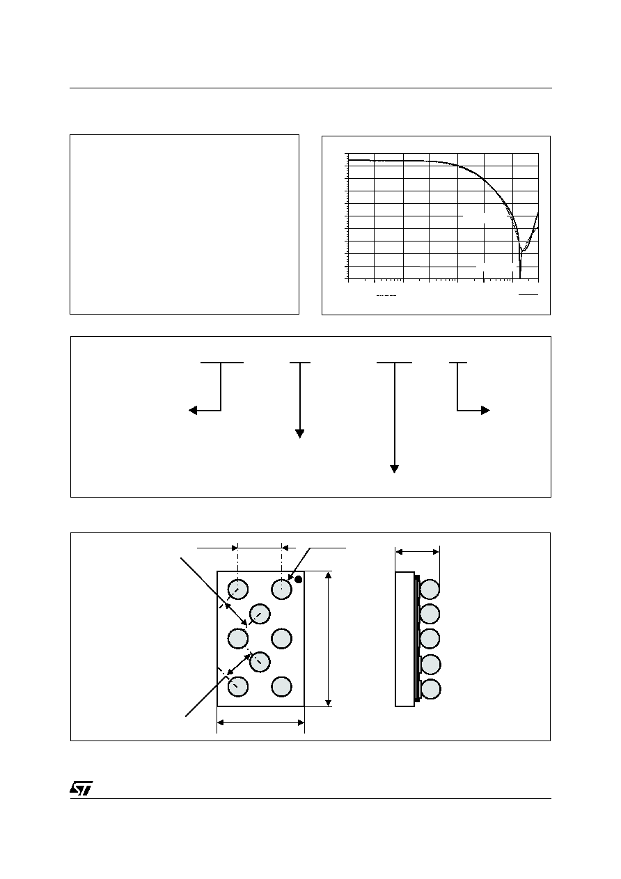
PACKAGE MECHANICAL DATA