BUL416
HIGH VOLTAGE FAST-SWITCHING
NPN POWER TRANSISTOR
s
SGS-THOMSON PREFERRED SALESTYPE
s
NPN TRANSISTOR
s
HIGH VOLTAGE CAPABILITY
s
VERY HIGH SWITCHING SPEED
s
FULLY CHARACTERISED AT 125
o
C
s
LOW SPREAD OF DYNAMIC PARAMETERS
APPLICATIONS
s
ELECTRONIC BALLASTS FOR
FLUORESCENT LIGHTING
s
SWITCH MODE POWER SUPPLIES
DESCRIPTION
The BUL416 is manufactured using high voltage
Multiepitaxial Mesa technology for cost-effective
high performance. It uses a Hollow Emitter
structure to enhance switching speeds.
The BUL series is designed for use in lighting
applications and low cost switch-mode power
supplies.
INTERNAL SCHEMATIC DIAGRAM
September 1997
ABSOLUTE MAXIMUM RATINGS
Symbol
Parameter
Val ue
Uni t
V
CES
Collect or-Emitt er Voltage (V
BE
= 0)
1600
V
V
CEO
Collect or-Emitt er Voltage (I
B
= 0)
800
V
V
EBO
Emitt er-Base Voltage (I
C
= 0)
9
V
I
C
Collect or Current
6
A
I
CM
Collect or Peak Current (t
p
< 5 ms)
9
A
I
B
Base Current
5
A
I
BM
Base Peak Current (t
p
< 5 ms)
8
A
P
t ot
Total Dissipation at T
c
= 25
o
C
110
W
T
stg
St orage Temperature
-65 to 150
o
C
T
j
Max. Operating Junction Temperature
150
o
C
1
2
3
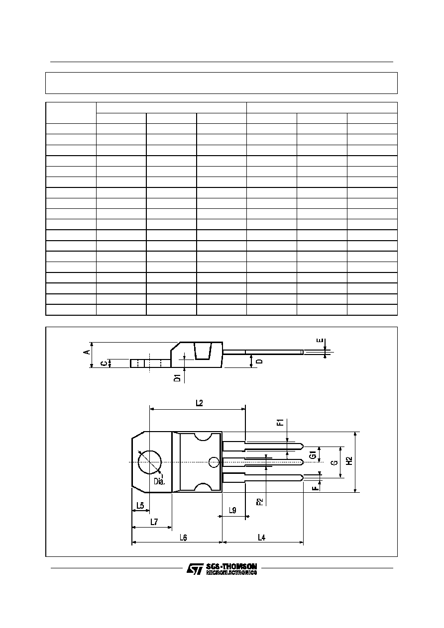
TO-220
1/6
THERMAL DATA
R
t hj-ca se
R
t hj- amb
Thermal Resistance Junction-Case
Max
Thermal Resistance Junction-Ambient
Max
1.14
62.5
o
C/W
o
C/W
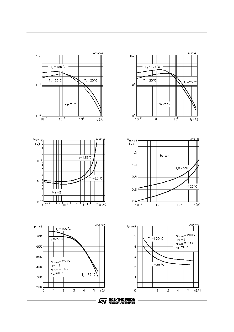
ELECTRICAL CHARACTERISTICS (T
case
= 25
o
C unless otherwise specified)
Symb ol
Parameter
Test Cond ition s
Mi n.
Typ .
Max.
Un it
I
CES
Collect or Cut-off
Current (V
BE
= 0)
V
CE
= 1600 V
V
CE
= 1600 V
T
j
= 125
o
C
100
500
�
A
�
A
I
CEO
Collect or Cut-off
Current (I
B
= 0)
V
CE
= 800 V
250
�
A
V
CEO (sus)
Collect or-Emitter
Sustaining Voltage
I
C
= 100 mA
L = 25 mH
800
V
V
EBO
Emitt er-Base Voltage
(I
C
= 0)
I
E
= 10 mA
9
V
V
CE(sat )
Collect or-Emitter
Saturat ion Voltage
I
C
= 2 A
I
B
= 0.4 A
I
C
= 4 A
I
B
= 1.33 A
1.5
3
V
V
V
BE(s at)
Base-Emitt er
Saturat ion Voltage
I
C
= 2 A
I
B
= 0.4 A
I
C
= 4 A
I
B
= 1.33 A
1.2
1.5
V
V
h
FE
DC Current G ain
I
C
= 0. 7 A
V
CE
= 5 V
I
C
= 10 mA
V
CE
= 5 V
12
10
40
t
s
t
f
INDUCTIVE LOAD
St orage Time
Fall T ime
I
C
= 3 A
I
B1
= 1 A
V
BE(of f)
= -5 V
R
BB
= 0
V
CL
= 200 V
L = 200
�
H
2.3
650
�
s
ns
t
s
t
f
INDUCTIVE LOAD
St orage Time
Fall T ime
I
C
= 3 A
I
B1
= 1 A
V
BE(of f)
= -5 V
R
BB
= 0
V
CL
= 200 V
L = 200
�
H
T
j
= 100
o
C
3
680
�
s
ns
Pulsed: Pulse duration = 300
�
s, duty cycle 1.5 %
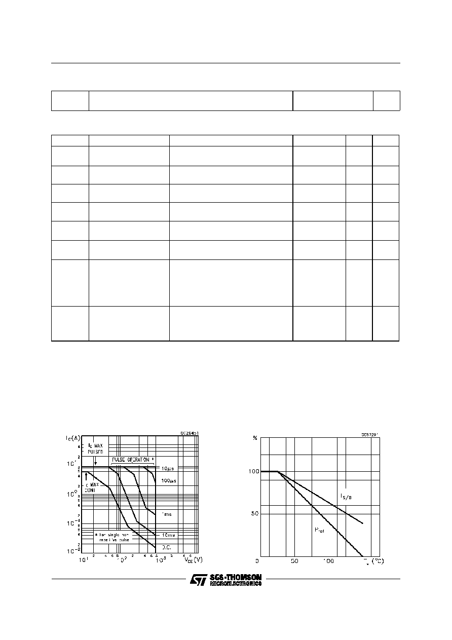
Safe Operating Areas
Derating Curve
BUL416
2/6
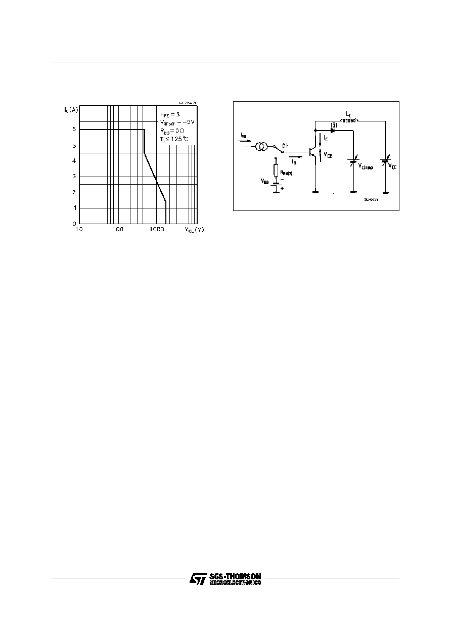
(1) Fast electronic switch
(2) Non-inductive Resistor
(3) Fast recovery rectifier
Reverse Biased SOA
RBSOA and Inductive Load Switching Test
Circuit
BUL416
4/6