BUH1215
HIGH VOLTAGE FAST-SWITCHING
NPN POWER TRANSISTOR
s
STMicroelectronics PREFERRED
SALESTYPE
s
HIGH VOLTAGE CAPABILITY
s
VERY HIGH SWITCHING SPEED
APPLICATIONS:
s
HORIZONTAL DEFLECTION FOR COLOUR
TV AND MONITORS
DESCRIPTION
The
BUH1215
is
manufactured
using
Multiepitaxial Mesa technology for cost-effective
high performance and uses a Hollow
Emitter
structure to enhance switching speeds.
The BUH series is designed for use in horizontal
deflection circuits in televisions and monitors.
®
INTERNAL SCHEMATIC DIAGRAM
January 1999
ABSOLUTE MAXIMUM RATINGS
Symbol
Parameter
Val ue
Uni t
V
CBO
Collector-Base Voltage (I
E
= 0)
1500
V
V
CEO
Collector-Emit ter Volt age (I
B
= 0)
700
V
V
EBO
Emitt er-Base Voltage (I
C
= 0)
10
V
I
C
Collector Current
16
A
I
CM
Collector Peak Current (t
p
< 5 ms)
22
A
I
B
Base Current
9
A
I
BM
Base Peak Current (t
p
< 5 ms)
12
A
P
t ot
Tot al Dissipation at T
c
= 25
o
C
200
W
T
stg
St orage Temperature
-65 to 150
o
C
T
j
Max. Operat ing Junction Temperat ure
150
o
C
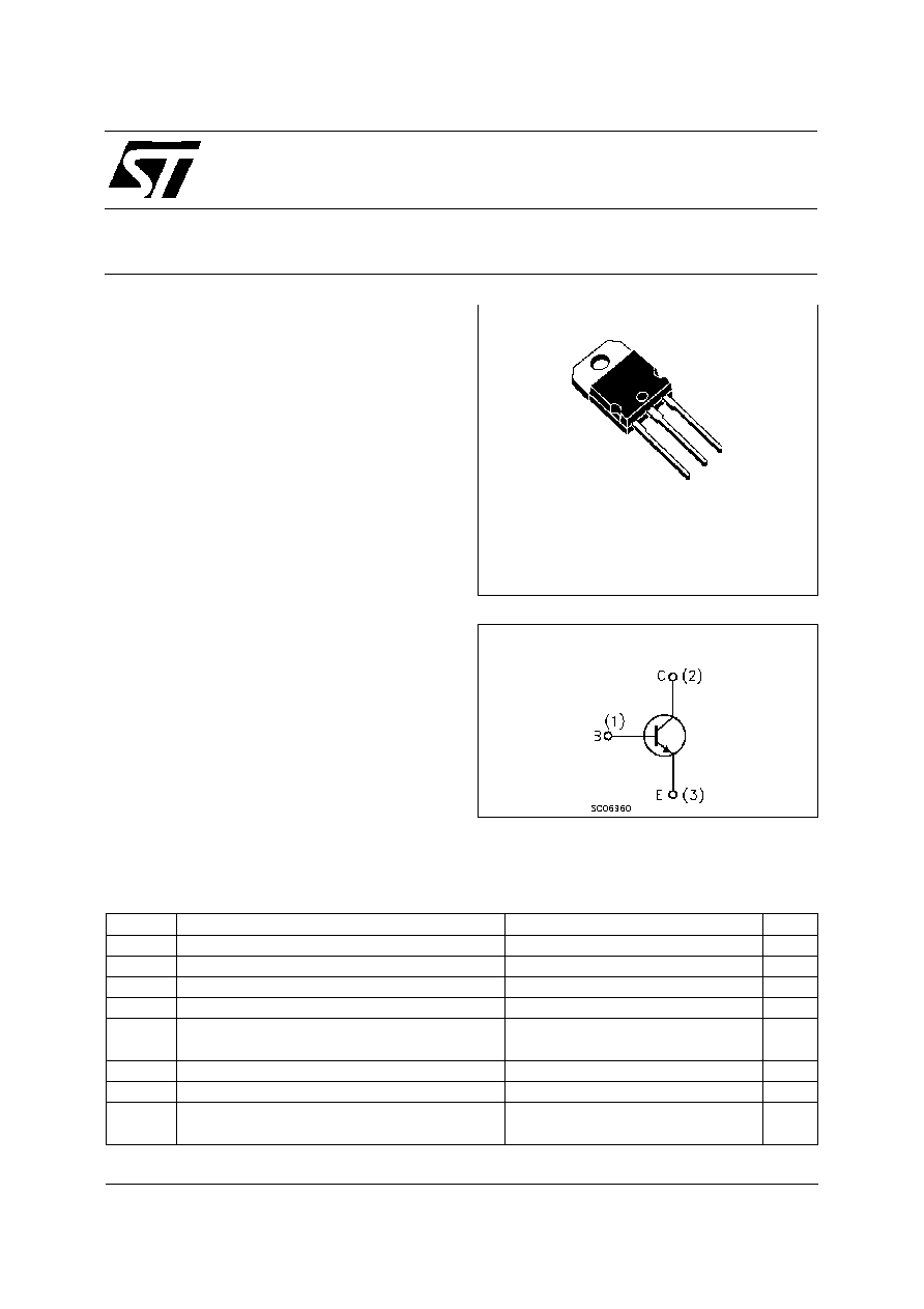
1
2
3
TO-218
1/7

THERMAL DATA
R
t hj-ca se
Thermal Resistance Junction-case
Max
0.63
o
C/W
ELECTRICAL CHARACTERISTICS (T
case
= 25
o
C unless otherwise specified)
Symb ol
Parameter
Test Cond ition s
Mi n.
Typ .
Max.
Un it
I
CES
Collector Cut -of f
Current (V
BE
= 0)
V
CE
= 1500 V
V
CE
= 1500 V
T
j
= 125
o
C
0.2
2
mA
mA
I
EBO
Emitt er Cut -of f Current
(I
C
= 0)
V
EB
= 5 V
100
ṁ
A
V
CEO (sus)
Collector-Emit ter
Sustaining Voltage
I
C
= 100 mA
700
V
V
EBO
Emitt er-Base Voltage
(I
C
= 0)
I
E
= 10 mA
10
V
V
CE(sat )
Collector-Emit ter
Saturation Voltage
I
C
= 12 A
I
B
= 2.4 A
1.5
V
V
BE(s at)
Base-Emitt er
Saturation Voltage
I
C
= 12 A
I
B
= 2.4 A
1.5
V
h
F E
DC Current Gain
I
C
= 12 A
V
CE
= 5 V
I
C
= 12 A
V
CE
= 5 V
T
j
= 100
o
C
7
5
10
14
t
s
t
f
RESI STIVE LO AD
St orage Time
Fall Time
V
CC
= 400 V
I
C
= 12 A
I
B1
= 2 A
I
B2
= -6 A
1.5
110
ṁ
s
ns
t
s
t
f
INDUCTIVE LO AD
St orage Time
Fall Time
I
C
= 12 A
f = 31250 Hz
I
B1
= 2 A
I
B2
= -1.5 A
V
c eflybac k
= 1050 sin
5
10
6
t
V
4
220
ṁ
s
ns
t
s
t
f
INDUCTIVE LO AD
St orage Time
Fall Time
I
C
= 6 A
f = 64 KHz
I
B1
= 1 A
V
BE(off )
= -2 A
V
c eflybac k
= 1200 sin
5
10
6
t
V
3.5
180
ṁ
s
ns
Pulsed: Pulse duration = 300
ṁ
s, duty cycle 1.5 %
Safe Operating Area
Thermal Impedance
BUH1215
2/7

Derating Curve
Collector Emitter Saturation Voltage
Power Losses at 64 KHz
DC Current Gain
Base Emitter Saturation Voltage
Switching Time Inductive Load at 64 KHz
(see figure 2)
BUH1215
3/7

Reverse Biased SOA
In order to saturate the power switch and reduce
conduction losses, adequate direct base current
I
B1
has to be provided for the lowest gain h
FE
at
100
o
C (line scan phase). On the other hand,
negative base current I
B2
must be provided the
transistor to turn off (retrace phase).
Most
of
the
dissipation, especially in
the
deflection application, occurs at switch-off so it is
essential to determine the value of I
B2
which
minimizes
power
losses,
fall
time
t
f
and,
consequently, T
j
. A new set of curves have been
defined to give total power losses, t
s
and t
f
as a
function of I
B1
at 64 KHz scanning frequencies for
choosing the optimum negative drive. The test
circuit is illustrated in figure 1.
The values of L and C are calculated from the
following equations:
1
2
L
(
I
C
)
2
=
1
2
C
(
V
CEfly
)
2
=
2
f
=
1
L
C
Where I
C
= operating collector current, V
CEfly
=
flyback voltage, f= frequency of oscillation during
retrace.
BASE DRIVE INFORMATION
BUH1215
4/7

Figure 1: Inductive Load Switching Test Circuits.
Figure 2: Switching Waveforms in a Deflection Circuit
BUH1215
5/7
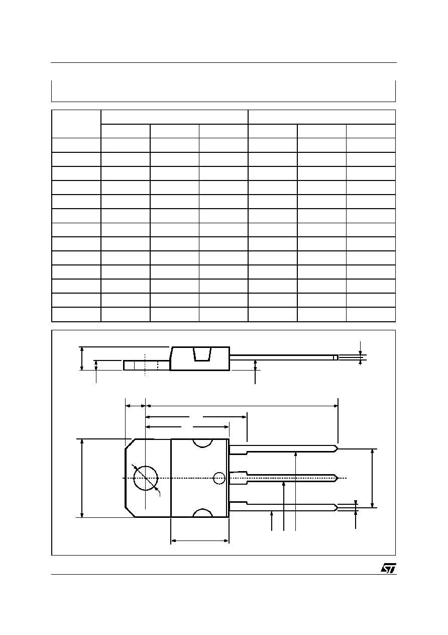
DIM.
mm
inch
MIN.
TYP.
MAX.
MIN.
TYP.
MAX.
A
4.7
4.9
0.185
0.193
C
1.17
1.37
0.046
0.054
D
2.5
0.098
E
0.5
0.78
0.019
0.030
F
1.1
1.3
0.043
0.051
G
10.8
11.1
0.425
0.437
H
14.7
15.2
0.578
0.598
L2
16.2
0.637
L3
18
0.708
L5
3.95
4.15
0.155
0.163
L6
31
1.220
R
12.2
0.480
Ø
4
4.1
0.157
0.161
R
A
C
D
E
H
F
G
L6
Ÿ
L3
L2
L5
1
2
3
TO-218 (SOT-93) MECHANICAL DATA
P025A
BUH1215
6/7

Information furnished is believed to be accurate and reliable. However, STMicroelectronics assumes no responsibility for the consequences
of use of such information nor for any infringement of patents or other rights of third parties which may result from its use. No license is
granted by implication or otherwise under any patent or patent rights of STMicroelectronics. Specification mentioned in this publication are
subject to change without notice. This publication supersedes and replaces all information previously supplied. STMicroelectronics products
are not authorized for use as critical components in life support devices or systems without express written approval of STMicroelectronics.
The ST logo is a trademark of STMicroelectronics
©
1999 STMicroelectronics Printed in Italy All Rights Reserved
STMicroelectronics GROUP OF COMPANIES
Australia - Brazil - Canada - China - France - Germany - Italy - Japan - Korea - Malaysia - Malta - Mexico - Morocco - The Netherlands -
Singapore - Spain - Sweden - Switzerland - Taiwan - Thailand - United Kingdom - U.S.A.
http://www.st.com
.
BUH1215
7/7