
BUF410
HIGH VOLTAGE FAST-SWITCHING
NPN POWER TRANSISTOR
s
SGS-THOMSON PREFERRED SALESTYPE
s
HIGH VOLTAGE CAPABILITY
s
VERY HIGH SWITCHING SPEED
s
MINIMUM LOT-TO-LOT SPREAD FOR
RELIABLE OPERATION
s
LOW BASE-DRIVE REQUIREMENTS
APPLICATIONS:
s
SWITCH MODE POWER SUPPLIES
s
MOTOR CONTROL
DESCRIPTION
The BUF410 is manufactured using High Voltage
Multi
Epitaxial
Planar
technology
for
high
switching speeds and high voltage capacity. They
use a Cellular Emitter structure with planar edge
termination to enhance switching speeds while
maintaining a wide RBSOA.
The
BUF
series
is
designed for
use
in
high-frequency power supplies and motor control
applications.
INTERNAL SCHEMATIC DIAGRAM
July 1997
ABSOLUTE MAXIMUM RATINGS
Symb ol
Parameter
Valu e
Un it
V
CEV
Collect or-Emitter Volt age (V
BE
= -1.5 V)
850
V
V
CEO
Collect or-Emitter Volt age (I
B
= 0)
450
V
V
EBO
Emitter-Base Volt age (I
C
= 0)
7
V
I
C
Collect or Current
15
A
I
CM
Collect or Peak Current (t
p
< 5 ms)
30
A
I
B
Base Current
3
A
I
BM
Base Peak Current (t
p
< 5 ms)
4.5
A
P
tot
T otal Dissipation at T
c
= 25
o
C
125
W
T
s tg
Storage Temperature
-65 to 150
o
C
T
j
Max O perat ion Junction Temperat ure
150
o
C
T
j
Max. Operating Junction T emperature
150
o
C
1
2
3
TO-218
1/6

THERMAL DATA
R
t hj-ca se
Thermal Resistance Junction-Case
Max
1
o
C/W
ELECTRICAL CHARACTERISTICS (T
case
= 25
o
C unless otherwise specified)
Symb ol
Parameter
Test Cond ition s
Mi n.
Typ .
Max.
Un it
I
CER
Collect or Cut-off
Current (R
BE
= 100
)
V
CE
= V
CEV
V
CE
= V
CEV
T
c
= 100
o
C
0.2
1
mA
mA
I
CEV
Collect or Cut-off
Current (I
B
= 0)
V
CE
= V
CEV
V
BE
= -1.5 V
V
CE
= V
CEV
V
BE
= -1.5 V T
c
=100
o
C
0.2
1
mA
mA
I
EBO
Emitt er Cut-off Current
(I
C
= 0)
V
BE
= 5 V
1
mA
V
CEO(sus )
Collect or-Emitter
Sustaining Voltage
I
C
= 200 mA
L = 25 mH
450
V
V
EBO
Emitt er Base Voltage
(I
C
= 0)
I
E
= 50 mA
7
V
V
CE(sat )
Collect or-Emitter
Saturat ion Voltage
I
C
= 5 A
I
B
= 0.5 A
I
C
= 5 A
I
B
= 0.5 A
T
c
=100
o
C
I
C
=10 A
I
B
= 2 A
I
C
=10 A
I
B
= 2 A
T
c
=100
o
C
0.8
0.5
2.8
2
V
V
V
V
V
BE(s at)
Base-Emitt er
Saturat ion Voltage
I
C
= 5 A
I
B
= 0.5 A
I
C
= 5 A
I
B
= 0.5 A
T
c
=100
o
C
I
C
=10 A
I
B
= 2 A
I
C
=10 A
I
B
= 2 A
T
c
=100
o
C
0.9
1.1
1.5
1.5
V
V
V
V
di
c
/dt
Rate of rise on-state
Collect or Current
V
CC
= 300 V R
C
= 0
t
p
= 3
µ
s
I
B1
= 0.75 A
T
j
=25
o
C
I
B1
= 0.75 A
T
j
=100
o
C
I
B1
= 3 A
T
j
=100
o
C
45
100
60
A
/µ
s
A
/µ
s
A
/µ
s
V
CE
(3
µ
s)
Collect or-Emitter
Dynamic Voltage
V
CC
= 300 V
R
C
= 60
I
B1
= 0.75 A
T
j
=25
o
C
I
B1
= 0.75 A
T
j
=100
o
C
2.1
8
V
V
V
CE
(5
µ
s)
Collect or-Emitter
Dynamic Voltage
V
CC
= 300 V
R
C
= 60
I
B1
= 0.75 A
T
j
=25
o
C
I
B1
= 0.75 A
T
j
=100
o
C
1.1
4
V
V
t
s
t
f
t
c
St orage Time
Fall T ime
Cross Over T ime
I
C
= 5 A
V
CC
= 50 V
V
BB
= - 5 V
R
BB
= 1. 2
V
c la mp
= 400 V
I
B1
= 0.5 A
L = 0.5 mH
0.8
0. 05
0. 08
µ
s
µ
s
µ
s
t
s
t
f
t
c
St orage Time
Fall T ime
Cross Over T ime
I
C
= 5 A
V
CC
= 50 V
V
BB
= - 5 V
R
BB
= 1. 2
V
c la mp
= 400 V
I
B1
= 0.5 A
L = 0.5 mH
T
j
=100
o
C
1.8
0.1
0.18
µ
s
µ
s
µ
s
V
CEW
Maximum Collect or
Emitt er Volt age
without Snubber
I
C
= 5 A
V
CC
= 50 V
V
BB
= - 5 V
R
BB
= 1. 2
V
c la mp
= 400 V
I
B1
= 0.5 A
L = 0.5 mH
T
j
=125
o
C
500
V
t
s
t
f
t
c
St orage Time
Fall T ime
Cross Over T ime
I
C
= 5 A
V
CC
= 50 V
V
BB
= 0
R
BB
= 0. 3
V
c la mp
= 400 V
I
B1
= 0.5 A
L = 0.5 mH
1.5
0. 04
0. 07
µ
s
µ
s
µ
s
BUF410
2/6

ELECTRICAL CHARACTERISTICS (continued)
Symb ol
Parameter
Test Cond ition s
Mi n.
Typ .
Max.
Un it
t
s
t
f
t
c
St orage Time
Fall T ime
Cross Over T ime
I
C
= 5 A
V
CC
= 50 V
V
BB
= 0
R
BB
= 0. 3
V
c la mp
= 400 V
I
B1
= 0.5 A
L = 0.5 mH
T
j
=100
o
C
3
0.15
0.25
µ
s
µ
s
µ
s
V
CEW
Maximum Collect or
Emitt er Volt age
without Snubber
I
C
= 5 A
V
CC
= 50 V
V
BB
= 0
R
BB
= 0.3
V
c la mp
= 400 V
I
B1
= 0.5 A
L = 0.5 mH
T
j
=125
o
C
500
V
t
s
t
f
t
c
St orage Time
Fall T ime
Cross Over T ime
I
C
= 10 A
V
CC
= 50 V
V
BB
= -5 V
R
BB
=1.2
V
c la mp
= 400 V
I
B1
= 2 A
L = 0.25 mH
1.9
0. 06
0. 12
µ
s
µ
s
µ
s
t
s
t
f
t
c
St orage Time
Fall T ime
Cross Over T ime
I
C
= 10 A
V
CC
= 50 V
V
BB
= - 5 V
R
BB
=1.2
V
c la mp
= 400 V
I
B1
= 2 A
L = 0.25 mH
T
j
=100
o
C
3.2
0.12
0.3
µ
s
µ
s
µ
s
V
CEW
Maximum Collect or
Emitt er Volt age
without Snubber
I
CW off
= 15 A
V
CC
= 50 V
V
BB
= - 5 V
R
BB
= 1. 2
L = 0.17 mH
I
B1
= 3 A
T
j
=125
o
C
400
V
Turn-on Switching Test Circuit
Turn-off Switching Test Circuit
Turn-on SwitchingTest Waveforms.
1) Fast electronic switch
2) Non-inductive Resistor
1) Fast electronic switch
2) Non-inductive Resistor
3) Fast recovery rectifier
BUF410
3/6
Turn-off SwitchingTest Waveforms (inductive load).
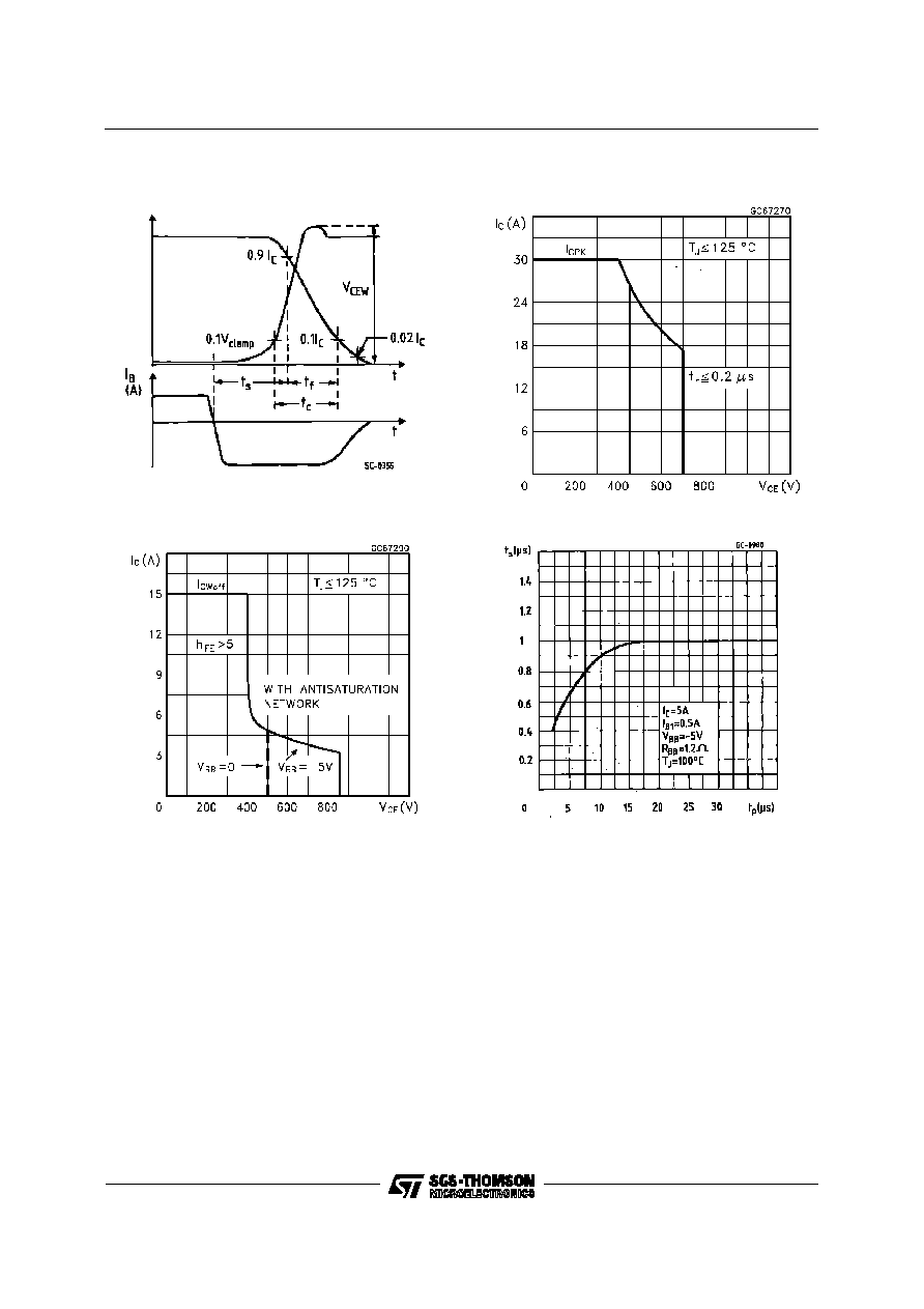
Forward Biased Safe Operating Areas.
Reverse Biased Safe Operating Area
Storage Time Versus Pulse Time.
BUF410
4/6

DIM.
mm
inch
MIN.
TYP.
MAX.
MIN.
TYP.
MAX.
A
4.7
4.9
0.185
0.193
C
1.17
1.37
0.046
0.054
D
2.5
0.098
E
0.5
0.78
0.019
0.030
F
1.1
1.3
0.043
0.051
G
10.8
11.1
0.425
0.437
H
14.7
15.2
0.578
0.598
L2
16.2
0.637
L3
18
0.708
L5
3.95
4.15
0.155
0.163
L6
31
1.220
R
12.2
0.480
Ř
4
4.1
0.157
0.161
R
A
C
D
E
H
F
G
L6
Ż
L3
L2
L5
1
2
3
TO-218 (SOT-93) MECHANICAL DATA
P025A
BUF410
5/6