10680 pixel
×
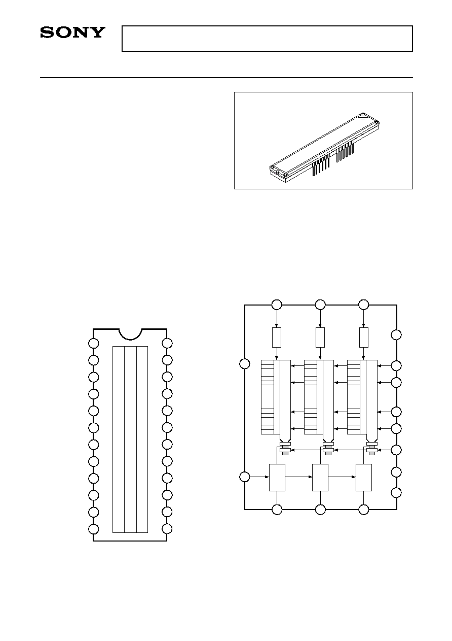
3 line CCD Linear Sensor (Color)
Description
The ILX550K is a reduction type CCD linear sensor
developed for color image scanner. This sensor reads
A4-size documents at a density of 1200DPI.
Features
· Number of effective pixels: 32040 pixels
(10680 pixels
×
3)
· Pixel size:
4µm
×
4µm (4µm pitch)
· Distance between line: 32µm (8 lines)
· Single-sided readout
· Ultra low lag/High sensitivity
· Single 12V power supply
· Maximum data rate:
5MHz/Color
· Input Clock Pulse:
CMOS 5V drive
· Number of output:
3 (R, G, B)
· Package:
24 pin Plastic DIP (400mil)
Absolute Maximum Ratings
· Supply voltage
V
DD
15
V
· Operating temperature
10 to +55
°C
Pin Configuration (Top View)
Block Diagram
1
E00420-PS
Sony reserves the right to change products and specifications without prior notice. This information does not convey any license by
any implication or otherwise under any patents or other right. Application circuits shown, if any, are typical examples illustrating the
operation of the devices. Sony cannot assume responsibility for any problems arising out of the use of these circuits.
ILX550K
24 pin DIP (Plastic)
D74
D75
S10680
Red
Read out gate
CCD register
D70
D69
S1
D18
D19
D74
D75
S10680
Green
Read out gate
CCD register
D70
D69
S1
D18
D19
D74
D75
S10680
Blue
Read out gate
CCD register
D70
D69
S1
D18
D19
Driver
16
ROG
-R
Driver
12
ROG
-G
Driver
13
ROG
-B
Output
amplifier
23
20
V
OUT-R
Output
amplifier
4
V
OUT-G
Output
amplifier
21
3
5
2
V
OUT-B
GND
10
GND
V
DD
RS
1
1
24
2
11
1
15
2
CLP
22
GND
1
2
3
4
5
6
7
8
9
10
11
12
13
14
15
16
17
18
19
20
21
22
23
24
1
RS
GND
V
OUT-G
10680
B
1
10680
G
1
10680
R
1
V
DD
NC
NC
NC
NC
GND
1
ROG
-G
2
CLP
GND
V
OUT-B
V
OUT-R
NC
NC
NC
ROG
-R
2
NC
ROG
-B
3
ILX550K
Unit
%
V
mV
mV
%
mA
%
V
Remarks
Note 3
Note 4
Note 8
Max.
3.6
4.5
3.5
20
--
--
--
--
5
12
--
50
--
--
--
Typ.
2.7
3.3
2.6
4
2.5
0.93
0.76
0.96
2
4
0.02
25
98
450
7.3
Min.
1.8
2.1
1.7
--
2
0.56
0.44
0.57
--
--
--
--
92
--
--
Symbol
R
R
R
G
R
B
PRNU
V
SAT
SE
R
SE
G
SE
B
V
DRK
DSNU
IL
I
VDD
TTE
Zo
V
OS
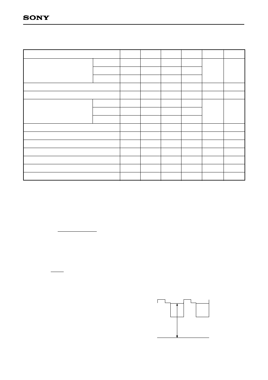
Item
Sensitivity nonuniformity
Saturation output voltage
Dark voltage average
Dark signal nonuniformity
Image lag
Supply current
Total transfer efficiency
Output impedance
Offset level
Electrooptical Characteristics (Note 1)
(Ta = 25°C, V
DD
= 12V, f
RS
= 1MHz, Input clock = 5Vp-p, Light source = 3200K, IR cut filter CM-500S (t = 1.0mm))
Notes)
1. In accordance with the given electrooptical characteristics, the black level is defined as the average value
of D18, D19 to D67.
2. For the sensitivity test light is applied with a uniform intensity of illumination.
3. PRNU is defined as indicated below. Ray incidence conditions are the same as for Note 2.
V
OUT-G
= 500mV (Typ.)
PRNU =
×
100 [%]
Where the 5340 pixels are divided into blocks of 100, the maximum output of each block is set to V
MAX
, the
minimum output to V
MIN
and the average output to V
AVE
.
4. Use below the minimum value of the saturation output voltage.
5. Saturation exposure is defined as follows.
SE =
Where R indicates R
R
, R
G
, R
B
, and SE indicates SE
R
, SE
G
, SE
B
.
6. Optical signal accumulated time
int stands at 5.5ms.
7. V
OUT-G
= 500mV (Typ.)
8. Vos is defined as indicated below.
V
OUT
indicates V
OUT-R
, V
OUT-G
and V
OUT-B
.
(V
MAX
V
MIN
)/2
V
AVE
V
SAT
R
Sensitivity
Saturation exposure
Red
Green
Blue
Red
Green
Blue
V/(lx · s)
Note 2
lx · s
Note 5
Note 6
Note 6
Note 7
V
OS
V
OUT
GND
,