CMOS-CCD 1H Delay Line for PAL
Description
The CXL5003M/P are general-purpose CMOS-CCD
delay line ICs that provide 1H delay time for PAL.
Features
· Low power consumption 110mW (Typ.)
· Small size package (8-pin SOP, DIP)
· Low differential gain DG = 3% (Typ.)
· Input signal amplitude 180 IRE (= 1.28Vp-p, Max.)
· Low input clock amplitude operation 150mVp-p (Min.)
· Built-in peripheral circuits (clock driver, timing
generator, autobias, and output circuits)
Functions
· 848-bit CCD register
· Clock drivers
· Autobias circuit
· Sync tip clamp circuit
· Sample and hold circuit
Structure
CMOS-CCD
Absolute Maximum Ratings (Ta = 25°C)
· Supply voltage
V
DD
11
V
· Supply voltage
V
CL
6
V
· Operating temperature
Topr 10 to +60
°C
· Storage temperature
Tstg 55 to +150 °C
· Allowable power dissipation
P
D
CXL5003M 350 mW
CXL5003P 480 mW
Recommended Operating Conditions
Supply voltage
V
DD
9 ± 5%
V
V
CL
5 ± 5%
V
Recommended Clock Conditions
· Input clock amplitude
V
CLK
150mVp-p to 1.0Vp-p
(250mVp-p typ.)
· Clock frequency
f
CLK
13.300856MHz
1
E51215B79-PS
Sony reserves the right to change products and specifications without prior notice. This information does not convey any license by
any implication or otherwise under any patents or other right. Application circuits shown, if any, are typical examples illustrating the
operation of the devices. Sony cannot assume responsibility for any problems arising out of the use of these circuits.
CXL5003M/P
CXL5003M
8 pin SOP (Plastic)
CXL5003P
8 pin DIP (Plastic)
3
CXL5003M/P
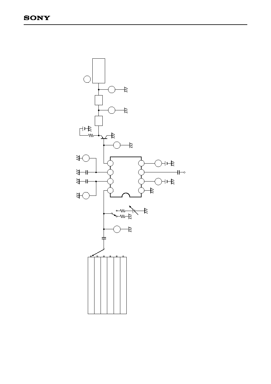
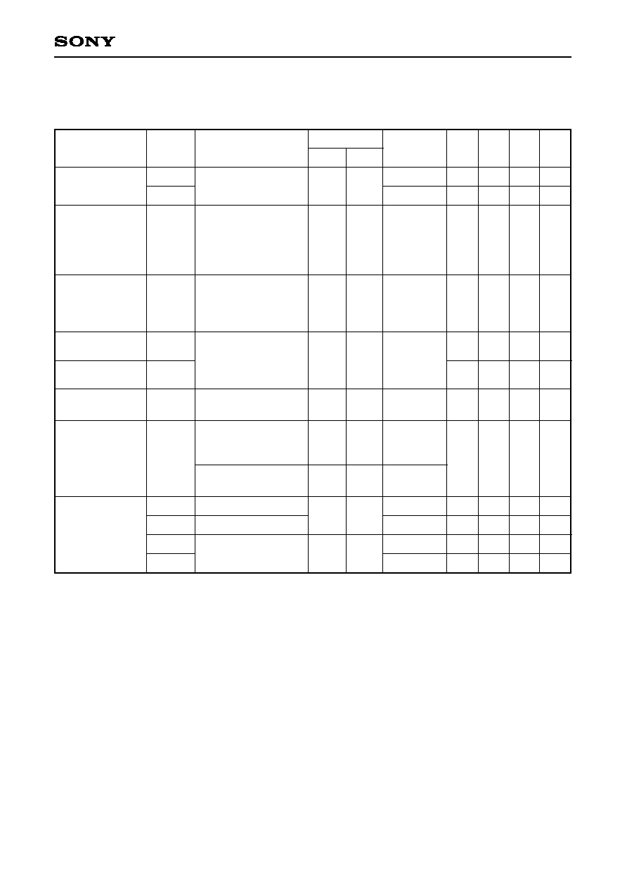
Electrical Characteristics
(Ta = 25°C, V
DD
= 9.0V, V
CL
= 5.0V, f
CLK
= 13.3MHz, V
CLK
= 250mVp-p sine wave,
See "Electrical characteristics test circuit")
Item
Symbol
Measuring condition
SW conditions
Measuring
point
Min.
Typ. Max. Unit
1
2
mA
mA
dB
dB
%
deg
Vp-p
dB
V
V
V
V
5
16
3
--
5
5
1.28
--
6.5
6.5
3.3
3.7
4
14
0
2.1
3
3
--
60
5.0
5.0
2.3
2.7
--
--
3
3.0
--
--
--
55
3.5
3.5
1.3
1.7
A1
A2
V1
V1
S
--
V2
V2
V3
V4
V5
V6
a
a
b
a
--
a
a
a
a
a
a
b, c
e
--
f
d
d
a
250kHz, 1.28Vp-p,
sine wave input
250kHz, 1.28Vp-p,
sine wave input
IG = 20 log (Output
voltage [Vp-p] /
1.28 [Vp-p])
Dissipation at 4.43MHz
in relation to 250kHz
fG = 20 log (V
4.43MHz
/
V
250kHz
) (Note 1)
5-staircase wave input
Y = 140 IRE (= 1.0Vp-p)
Measure S point with
vector scope (Note 2)
S: Input = 250kHz,
1.0Vp-p
output (Vp-p)
N: Input = DC ground
output (mVrms)
250kHz, 1.28Vp-p,
sine wave input
I
DD
I
CL
IG
fG
DG
DP
V
IN-AC
S/N
V
IN-AC
V
AUTO-DC
V
FEED-DC
V
OUT-DC
Supply current
Insertion gain
Frequency
response
Differential gain
Differential phase
Allowable input
amplitude
Noise
Output DC
voltage
5
CXL5003M/P
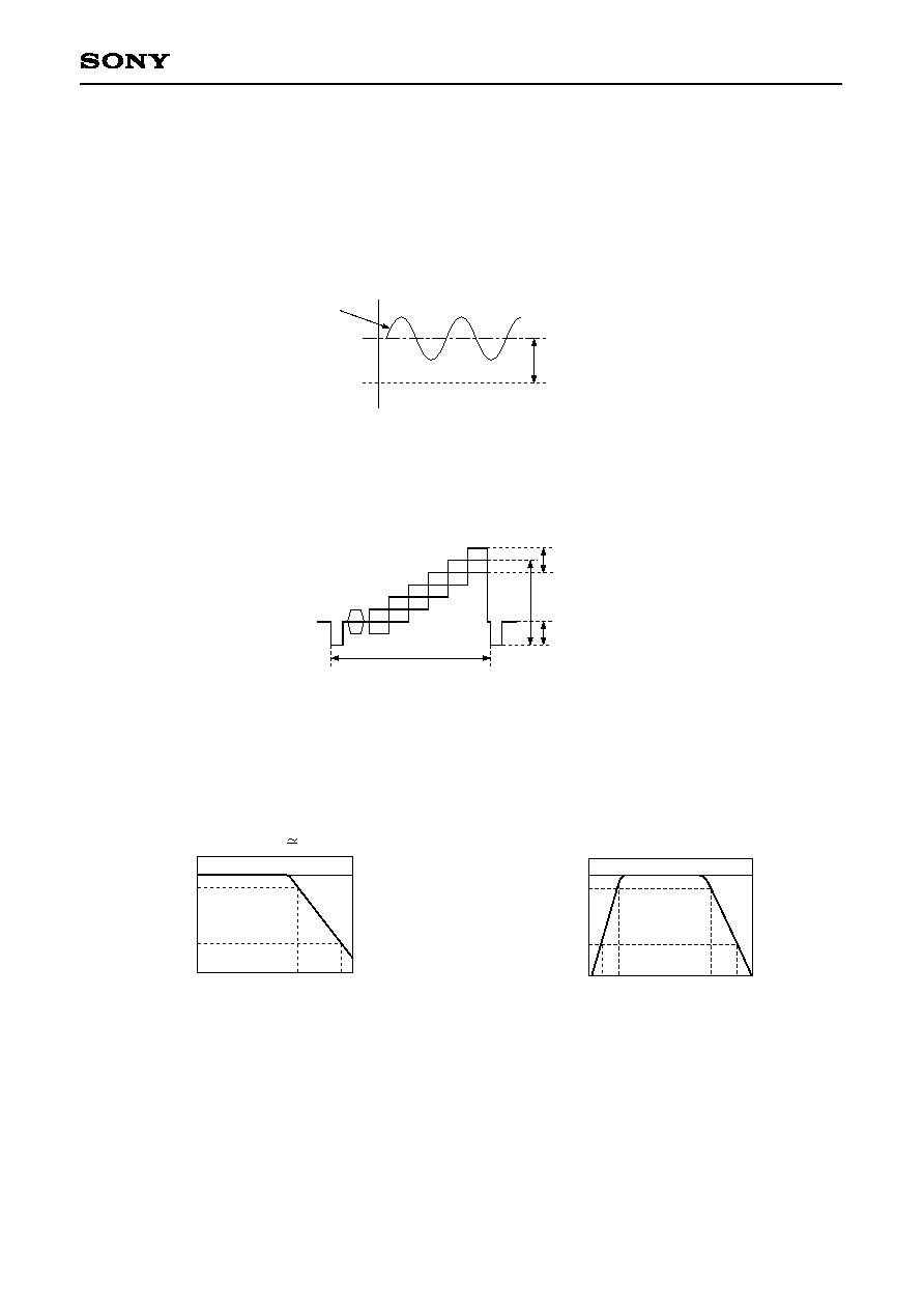
Note 1) Frequency response measuring condition
V
4.43MHz
(Output signal voltage [Vp-p] at 4.43MHz input)
V
250kHz
(Output signal voltage [Vp-p] at 250kHz input)
Set Pin 8 (IN) voltage [V] = V
IN-DC
+ 640mV.
4.43MHz, 300mVp-p sine wave
250kHz, 300mVp-p sine wave
640mV (adjust with V
BIAS
)
V
IN-DC
[V]
Note 2) Differential gain and differential phase measuring condition
1H 64.0µs
40 IRE
140 IRE (1.0Vp-p)
Chroma 40 IRE
5-staircase wave signal
DG and DP are measured at output S point by vector scope.
Note 3) LPF frequency response
0
5.8
13.3
Frequency [MHz]
50
3
0
[dB]
(Delay time 170ns)
Note 4) BPF frequency response
0
5.1M 13.3M
Frequency [Hz]
50
3
0
[dB]
200
50