Description
The CXK77B3611AGB-5/6 is a high speed 1M bit
Bi-CMOS synchronous static RAM organized as
32768 words by 36 bits. This SRAM integrates input
registers, high speed SRAM and write buffer onto a
single monolithic IC and features the delayed write
system to reduce the dead cycles.
Features
· Fast cycle time
(Cycle)
(Frequency)
CXK77B3611AGB-5
5ns
200MHz
-6
6ns
167MHz
· Inputs and outputs are GTL/HSTL compatible
· Controlled Impedance Driver
· Single 3.3V power supply: 3.3V±0.15V
· Byte-write possible
· OE asynchronization
· JTAG test circuit
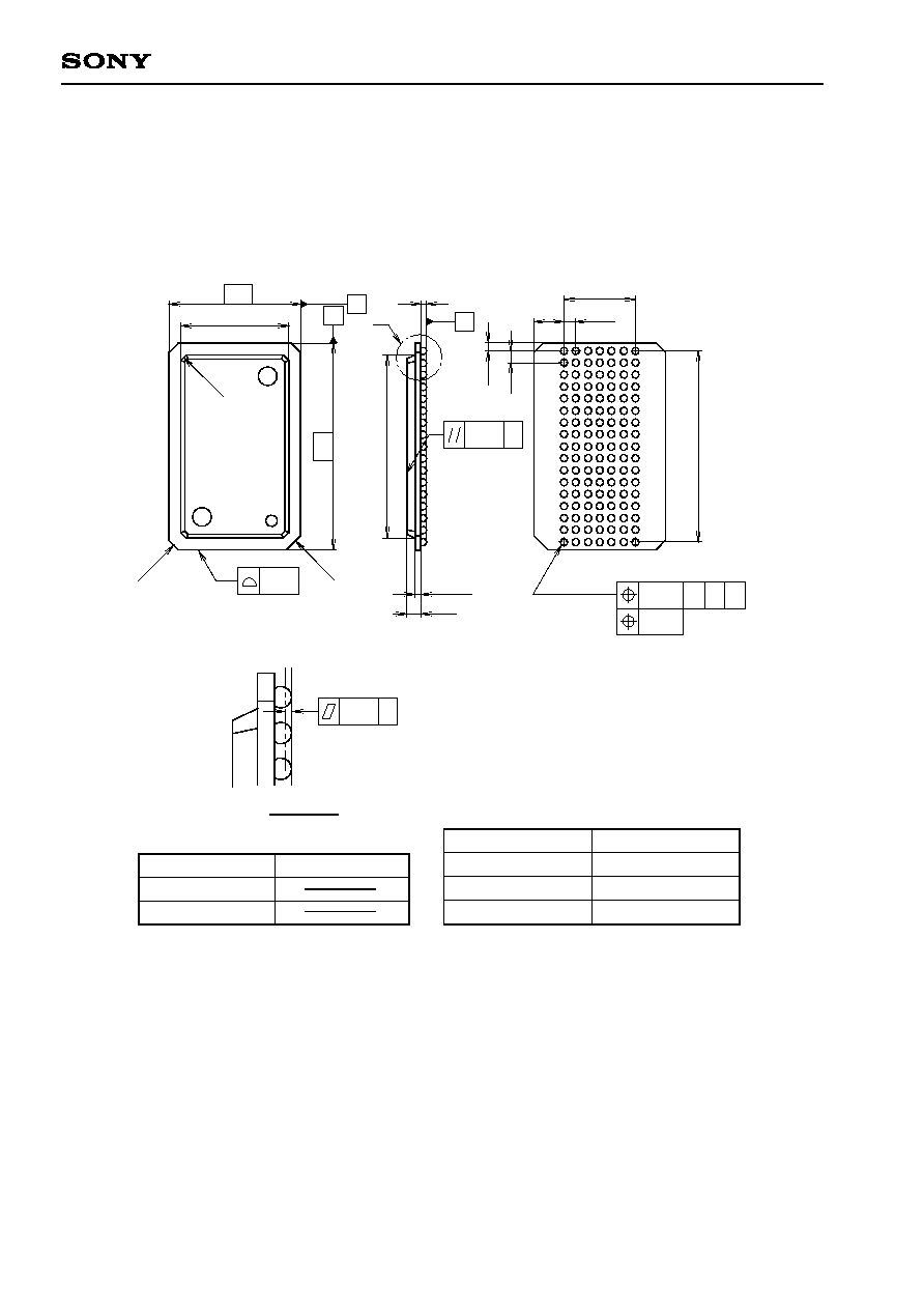
· Package 119TBGA
· 4 kinds of synchronous operation mode
Register-Register mode (R-R mode)
Register-Flow Thru mode (R-F mode)
Register-Latch mode (R-L mode)
Dual clock mode (D-C mode)
Function
32768 word x 36bit High Speed Bi-CMOS Synchronous SRAM
Structure
Silicon gate Bi-CMOS IC
1
CXK77B3611AGB
-5/6
119 pin BGA (Plastic)
PE96812
High Speed Bi-CMOS Synchronous Static RAM
Sony reserves the right to change products and specifications without prior notice. This information does not convey any license by
any implication or otherwise under any patents or other right. Application circuits shown, if any, are typical examples illustrating the
operation of the devices. Sony cannot assume responsibility for any problems arising out of the use of these circuits.
Preliminary
For the availability of this product, please contact the sales office.
3
CXK77B3611AGB
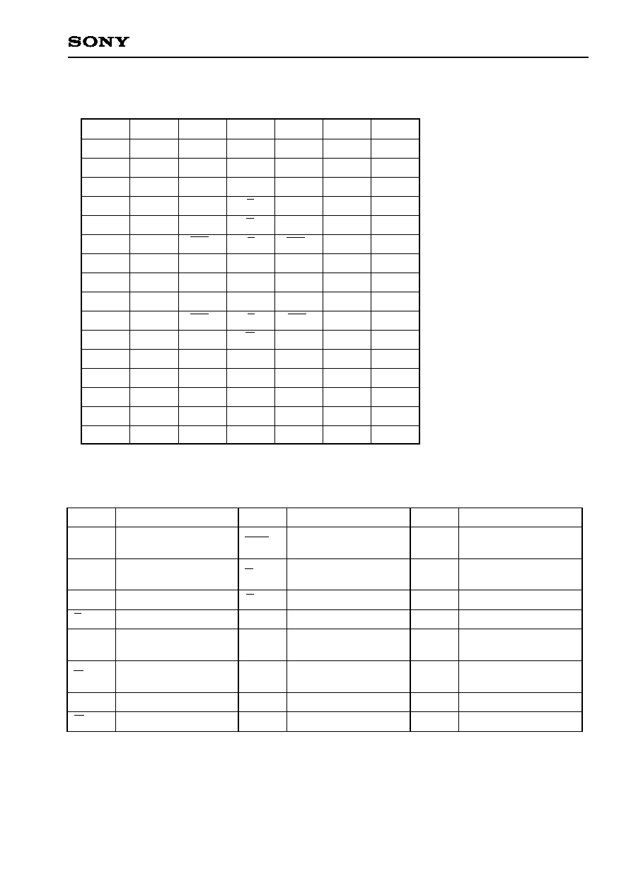
Pin Configuration (Top View)
V
DD
Q
NC
NC
DQc
DQc
V
DD
Q
DQc
DQc
V
DD
Q
DQd
DQd
V
DD
Q
DQd
DQd
NC
NC
V
DD
Q
A
B
C
D
E
F
G
H
J
K
L
M
N
P
R
T
U
A
NC
A
DQc
DQc
DQc
DQc
DQc
V
DD
DQd
DQd
DQd
DQd
DQd
A
NC
TMS
A
NC
A
V
SS
V
SS
V
SS
BWc
V
SS
VREF
V
SS
BWd
V
SS
V
SS
V
SS
M1
A
TDI
NC
NC
V
DD
ZQ
S
G
C
C
V
DD
K
K
W
A
A
V
DD
A
TCK
A
NC
A
V
SS
V
SS
V
SS
BWb
V
SS
VREF
V
SS
BWa
V
SS
V
SS
V
SS
M2
A
TDO
A
NC
A
DQb
DQb
DQb
DQb
DQb
V
DD
DQa
DQa
DQa
DQa
DQa
A
NC
NC
V
DD
Q
NC
NC
DQb
DQb
V
DD
Q
DQb
DQb
V
DD
Q
DQa
DQa
V
DD
Q
DQa
DQa
NC
ZZ
V
DD
Q
1
2
3
4
5
6
7
Pin Description
A
DQx
K
K
C
C
VREF
W
Address Input
Data I/O in byte
(a to d)
Positive Clock
Negative Clock
Output Positive Clock(
)
Output Negative
Clock(
)
Input Reference
Write Enable
BWX
S
G
ZZ
TCK
TMS
TDI
TDO
Byte Write Enable
(a to d)
Chip Select
Asyn Output Enable
Sleep Mode Select
JTAG Clock
JTAG Mode Select
JTAG Data In
JTAG Data Out
V
DD
V
DD
Q
V
SS
M1, M2
ZQ
NC
+3.3V power supply
Output power supply
Ground
Mode Select
Output Impedance
Control
No Connect
Symbol
Description
Symbol
Description
Symbol
Description
(
) These pins should be tied to V
DD
or V
SS
except D-C mode.