
1
E02561-PS
Sony reserves the right to change products and specifications without prior notice. This information does not convey any license by
any implication or otherwise under any patents or other right. Application circuits shown, if any, are typical examples illustrating the
operation of the devices. Sony cannot assume responsibility for any problems arising out of the use of these circuits.
CXD3611R
64 pin LQFP (Plastic)
Timing Generator for Progressive Scan CCD Image Sensor
Description
The CXD3611R is a timing generator IC which
generates the timing pulses for performing progressive
scan readout using the ICX414/415/424 CCD image
sensors.
Features
· Base oscillation frequency
24.545451MHz (ICX414, 424)/
29.500000MHz (ICX415)
(When in double speed drive mode:
49.090902/59.000000MHz)
· Electronic shutter function
· Trigger shutter function
· Supports central scanning mode (two types)/
double speed drive mode
· Horizontal driver for CCD image sensor
(However, uses external driver for double speed
drive mode.)
· Vertical driver for CCD image sensor
Applications
Monitoring/image analysis
Structure
Silicon gate CMOS IC
Applicable CCD Image Sensors
· ICX414 (Type 1/2, 330K pixels)
· ICX415 (Type 1/2, 460K pixels)
· ICX424 (Type 1/3, 330K pixels)
Absolute Maximum Ratings
· Supply voltage V
DD
Vss 0.3 to +7.0
V
VL
10.0 to Vss
V
VH
VL 0.3 to +26.0
V
· Input voltage
V
I
Vss 0.3 to V
DD
+ 0.3
V
· Output voltage V
O1
Vss 0.3 to V
DD
+ 0.3
V
V
O2
V
L
0.3 to V
SS
+ 0.3
V
V
O3
V
L
0.3 to V
H
+ 0.3
V
· Operating temperature
Topr
20 to +75
°C
· Storage temperature
Tstg
55 to +150
°C
Recommended Operating Conditions
· Supply voltage V
DD
a, V
DD
b
3.0 to 5.5
V
V
DD
c
3.0 to 3.6
V
VM
0.0
V
VH
14.5 to 15.5
V
VL
7.0 to 8.0
V
· Operating temperature
Topr
20 to +75
°C
2
CXD3611R
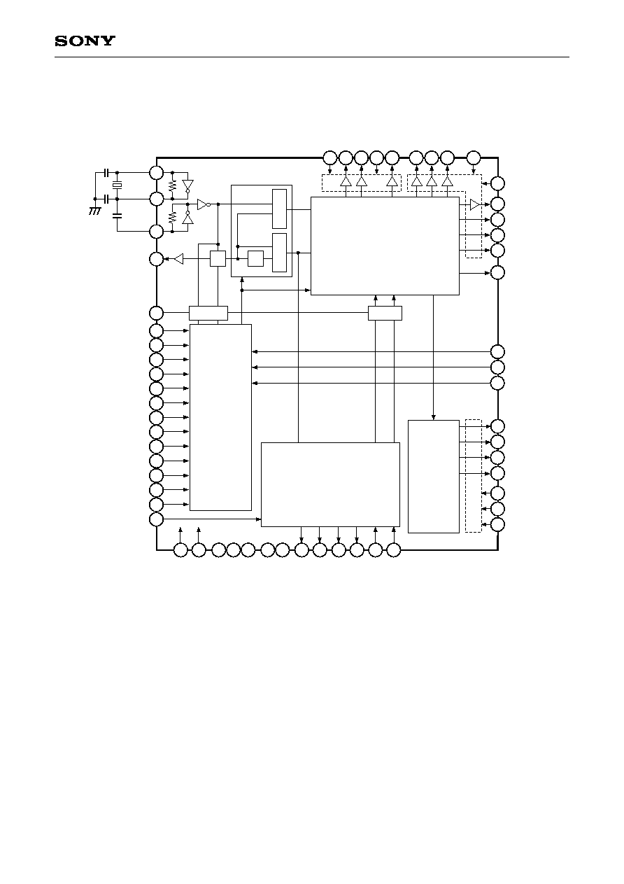
Block Diagram
Notes) 1. CKI must always be input below amplitude V
DD
with a sine wave.
2. The system block diagram above is an example using an oscillator.
45
44
58
62
54
52
41
24
23
26
32
31
30
29
V2
V3
SUB
V1
36
35
34
TRG
ESG
RDM
WEN
V
SS
3
CLPDM
PBLK
ADCLK
HDI
VDI
47
46
VDO
HDO
MCKO
CKI
OSCO
OSCI
Pulse Generator
25 OBCLP
60
56
50
VL
VH
VM
9
10
SMD3
SMD2
7
8
SMD1
MD3
5
6
MD2
MD1
12
4
CCD
CDSRS
37
11
HDRS
PS
39
40
SEN
SCK
2
38
SSI
SNCSL
V Driver
Register
3
SSGSL
1/2
1/2
14
18
RG
V
DD
2
19
22
21
20
V
DD
3
XRS
XSHD
XSHP
17
16
15
H2
H1
Vss2
Latch
27
SSG
49
64
TEST
RST
43
42
BLK
SYNC
13 33
V
DD
4
V
DD
1
28 48
Vss5
Vss4
1
Vss1
Selector
Selector
Selector
3
CXD3611R
Groups of pins enclosed in the figure indicate sections for which power supply separation is possible.
1
2
3
4
5
6
7
8
9
10
11
12
21
22
23
24
25
26
27
28
29
30
31
32
37
38
39
40
41
42
43
44
45
46
47
48
49
50
51
52
53
54
55
56
57
58
59
60
XSHD
XRS
PBLK
CLPDM
OBCLP
ADCLK
Vss3
Vss4
MCKO
CKI
OSCO
OSCI
PS
SSI
SCK
SEN
WEN
BLK
SYNC
HDI
VDI
VDO
HDO
V
SS
5
CDSRS
HDRS
SMD3
SMD2
SMD1
13
14
15
16
33
34
35
36
V
DD
4
RDM
TRG
ESG
H1
V
SS
2
RG
V
DD
1
MD2
MD3
MD1
CCD
SSGSL
SNCSL
V
SS
1
VL
NC
V3
NC
VH
17
18
19
20
61
62
63
64
H2
V
DD
2
V
DD
3
XSHP
TEST
NC
SUB
NC
NC
V2
NC
V1
NC
VM
RST
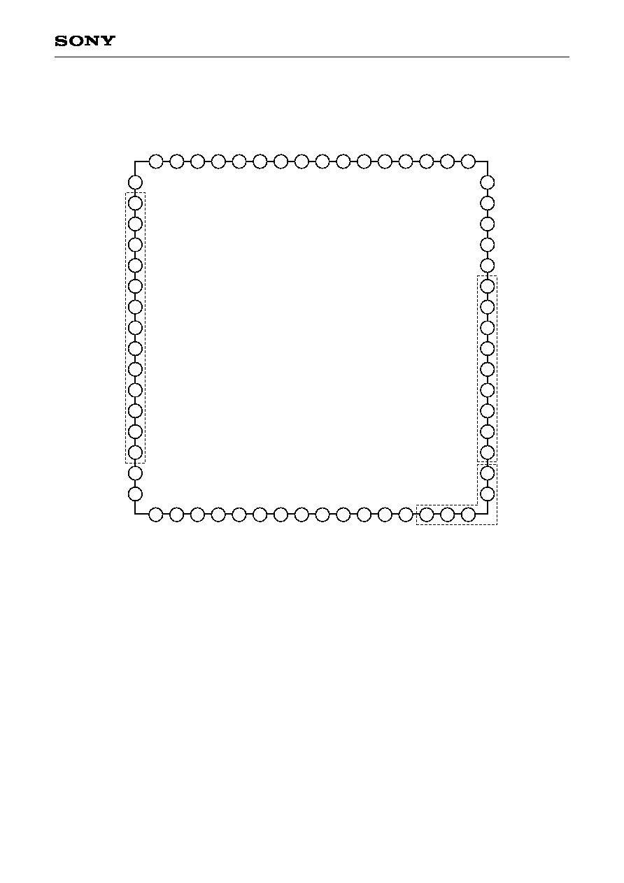
Pin Configuration
4
CXD3611R
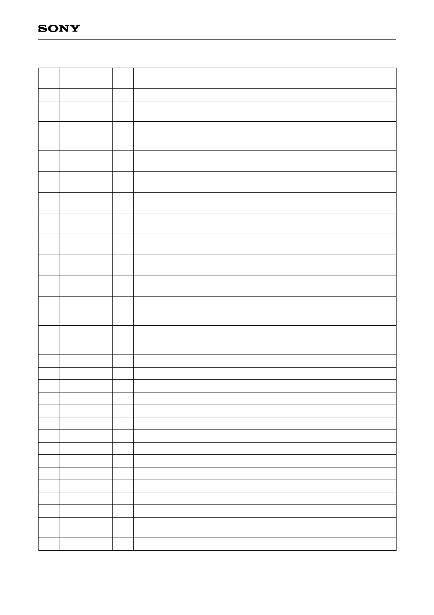
Pin Description
Pin
No.
1
2
3
4
5
6
7
8
9
10
11
12
13
14
15
16
17
18
19
20
21
22
23
24
25
26
27
Symbol
V
SS
1
SNCSL
SSGSL
CCD
MD1
MD2
MD3
SMD1
SMD2
SMD3
HDRS
CDSRS
V
DD
1
RG
V
SS
2
H1
H2
V
DD
2
V
DD
3
XSHP
XSHD
XRS
PBLK
CLPDM
OBCLP
ADCLK
V
SS
3
I/O
--
I
I
I
I
I
I
I
I
I
I
I
--
O
--
O
O
--
--
O
O
O
O
O
O
O
--
Description
GND
Control input used to switch sync system
High: CKI sync, Low: MCKO sync.
With pull-down resistor
Pin used to switch external reset
High: External sync has priority, Low: Internal sync has priority
With pull-down resistor
Control input used to switch CCD
High: ICX415, Low: ICX414/424
With pull-down resistor
Control input 1 used to switch drive mode
See the section on parallel control
With pull-down resistor
Control input 2 used to switch drive mode
See the section on parallel control
With pull-down resistor
Control input 3 used to switch drive mode
See the section on parallel control
With pull-down resistor
Control input 1 used to switch exposure time
See the section on parallel control
With pull-down resistor
Control input 2 used to switch exposure time
See the section on parallel control
With pull-down resistor
Control input 3 used to switch exposure time
See the section on parallel control
With pull-down resistor
Control input used to switch H system pulse polarity
H1 and H2 are targeted (Default is positive polarity.)
High: For external Dr, Low: For internal Dr
With pull-down resistor
Control input used to switch CDS system pulse polarity
XSHP, XSHD, XRS, OBCLP, CLPDM are targeted.
High: Positive polarity, Low: Negative polarity
With pull-down resistor
3.3V power supply. (Power supply for common logic block)
CCD reset gate pulse output
GND
CCD horizontal register clock output
CCD horizontal register clock output
3.3V power supply. (Power supply for H1/H2/RG)
3.3V power supply. (Power supply for CDS)
CCD precharge level sample-and-hold pulse output
CCD data level sample-and-hold pulse output
Sample-and-hold pulse output for analog/digital conversion phase alignment
Pulse output for horizontal and vertical blanking period pulse cleaning
CCD dummy signal clamp pulse output
CCD optical black signal clamp pulse output
Clock output for analog/digital conversion IC
Logical phase can be adjusted using serial interface data.
GND
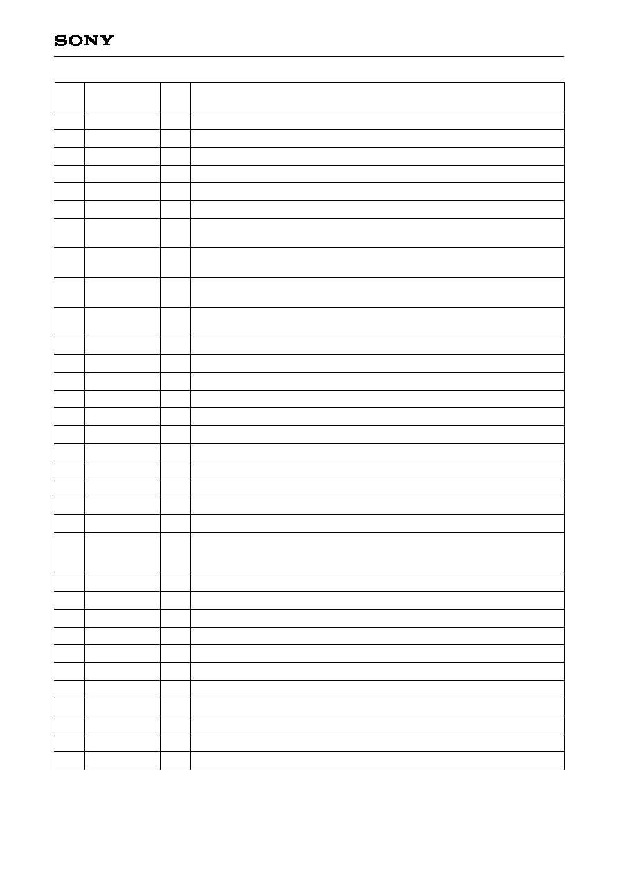
5
CXD3611R
Pin
No.
28
29
30
31
32
33
34
35
36
37
38
39
40
41
42
43
44
45
46
47
48
49
50
51
52
53
54
55
56
57
58
59
60
Symbol
V
SS
4
MCKO
CKI
OSCO
OSCI
V
DD
4
RDM
TRG
ESG
PS
SSI
SCK
SEN
WEN
BLK
SYNC
HDI
VDI
VDO
HDO
V
SS
5
RST
VM
NC
VI
NC
V2
NC
VH
NC
V3
NC
VL
I/O
--
O
I
O
I
--
I
I
I
I
I
I
I
O
O
O
I
I
O
O
--
I
--
--
O
--
O
--
--
--
O
--
--
Description
GND
System clock output for signal processing IC
Inverter input
Inverter output for oscillation; should be open or C grounded when not in use.
Inverter input for oscillation; should be fixed to Low when not in use.
3.3V power supply. (Power supply for common logic block)
Trigger control, normally fixed to V
DD
.
See the section on trigger shutter function.
With pull-up resistor
Trigger control, normally fixed to V
DD
.
See the section on trigger shutter function.
With pull-up resistor
Readout pulse position control, normally fixed to V
DD
.
See the section on trigger shutter function.
With pull-up resistor
Control input used to switch serial and parallel
High: Parallel, Low: Serial
With pull-up resistor
Serial interface data input for internal mode settings.
Schmitt trigger input
Serial interface clock input for internal mode settings.
Schmitt trigger input
Serial interface strobe input for internal mode settings.
Schmitt trigger input
Memory writing timing pulse output
Blank pulse output
SYNC pulse output
Horizontal sync reset signal input
With pull-up resistor
Vertical sync reset signal input
With pull-up resistor
Vertical sync signal output
Horizontal sync signal output
GND
Input pin for internal system reset
Normally, apply reset during power-on.
High: Normal operation, Low: Reset control
Schmitt trigger input
GND (Ground for vertical driver)
No connection
CCD vertical register clock output
No connection
CCD vertical register clock output
No connection
15.0V power supply. (Power supply for vertical driver)
No connection
CCD vertical register clock output
No connection
7.5V power supply. (Power supply for vertical driver)